Analog-to-Digital Converter (ADC10B16CV2)
MC9S12G Family Reference Manual Rev.1.27
NXP Semiconductors 513
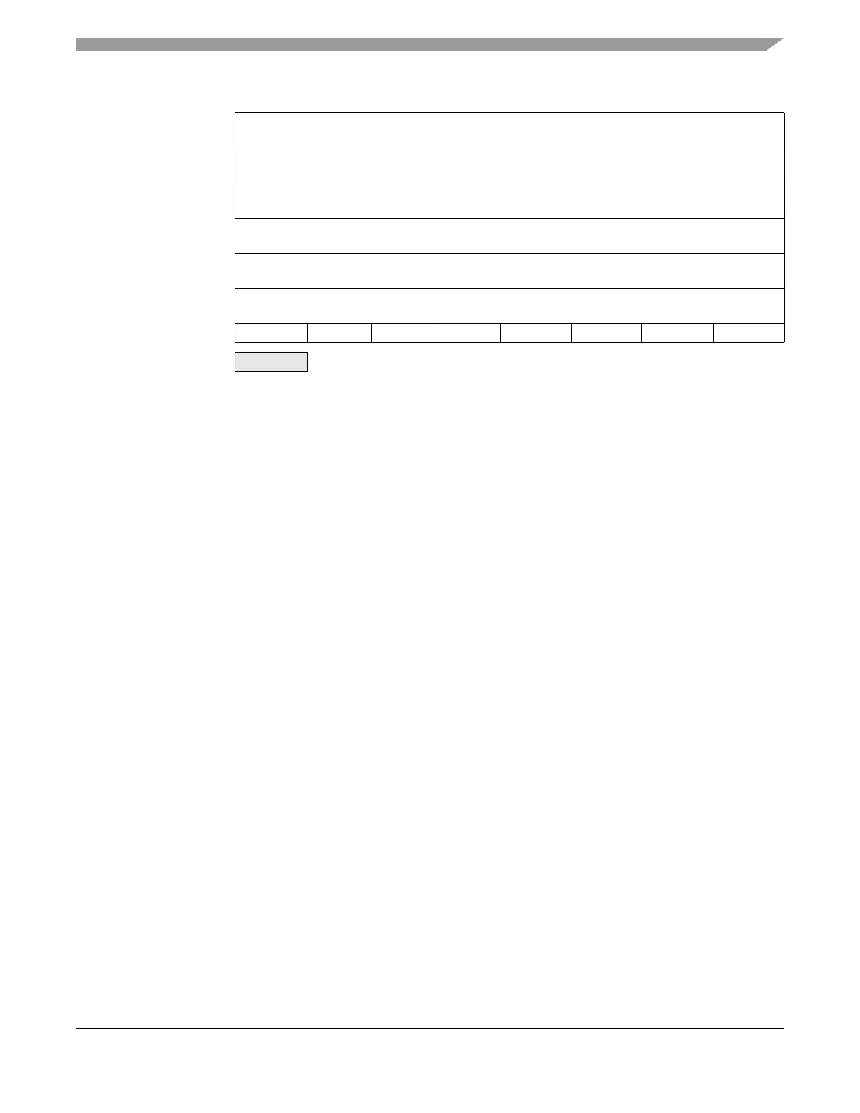
0x0024 ATDDR10
R
See Section 15.3.2.12.1, “Left Justified Result Data (DJM=0)”
and Section 15.3.2.12.2, “Right Justified Result Data (DJM=1)”
W
0x0026 ATDDR11
R
See Section 15.3.2.12.1, “Left Justified Result Data (DJM=0)”
and Section 15.3.2.12.2, “Right Justified Result Data (DJM=1)”
W
0x0028 ATDDR12
R
See Section 15.3.2.12.1, “Left Justified Result Data (DJM=0)”
and Section 15.3.2.12.2, “Right Justified Result Data (DJM=1)”
W
0x002A ATDDR13
R
See Section 15.3.2.12.1, “Left Justified Result Data (DJM=0)”
and Section 15.3.2.12.2, “Right Justified Result Data (DJM=1)”
W
0x002C ATDDR14
R
See Section 15.3.2.12.1, “Left Justified Result Data (DJM=0)”
and Section 15.3.2.12.2, “Right Justified Result Data (DJM=1)”
W
0x002E ATDDR15
R
See Section 15.3.2.12.1, “Left Justified Result Data (DJM=0)”
and Section 15.3.2.12.2, “Right Justified Result Data (DJM=1)”
W
W
Address Name Bit 7 6 5 4 3 2 1 Bit 0
= Unimplemented or Reserved
Figure 15-2. ADC10B16C Register Summary (Sheet 3 of 3)

 Loading...


