Analog-to-Digital Converter (ADC12B16CV2)
MC9S12G Family Reference Manual Rev.1.27
542 NXP Semiconductors
16.3.2.3 ATD Control Register 2 (ATDCTL2)
Writes to this register will abort current conversion sequence.
Read: Anytime
Write: Anytime
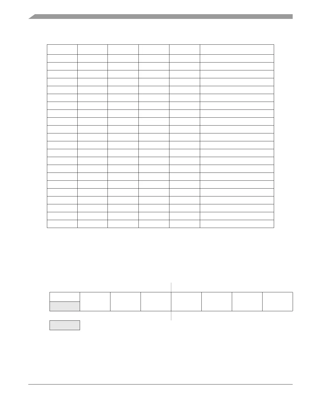
Table 16-5. External Trigger Channel Select Coding
ETRIGSEL ETRIGCH3 ETRIGCH2 ETRIGCH1 ETRIGCH0 External trigger source is
00000 AN0
00001 AN1
00010 AN2
00011 AN3
00100 AN4
00101 AN5
00110 AN6
00111 AN7
01000 AN8
01001 AN9
01010 AN10
01011 AN11
01100 AN12
01101 AN13
01110 AN14
01111 AN15
10000 ETRIG0
1
1
Only if ETRIG3-0 input option is available (see device specification), else ETRISEL is ignored, that means
external trigger source is still on one of the AD channels selected by ETRIGCH3-0
10001 ETRIG1
1
10010 ETRIG2
1
10011 ETRIG3
1
101XX Reserved
11XXX Reserved
Module Base + 0x0002
76543210
R0
AFFC Reserved ETRIGLE ETRIGP ETRIGE ASCIE ACMPIE
W
Reset00000000
= Unimplemented or Reserved
Figure 16-5. ATD Control Register 2 (ATDCTL2)

 Loading...


