Analog-to-Digital Converter (ADC12B16CV2)
MC9S12G Family Reference Manual Rev.1.27
NXP Semiconductors 555
16.3.2.12.2 Right Justified Result Data (DJM=1)
Table 16-22 shows how depending on the A/D resolution the conversion result is transferred to the ATD
result registers for right justified data. Compare is always done using all 12 bits of both the conversion
result and the compare value in ATDDRn.
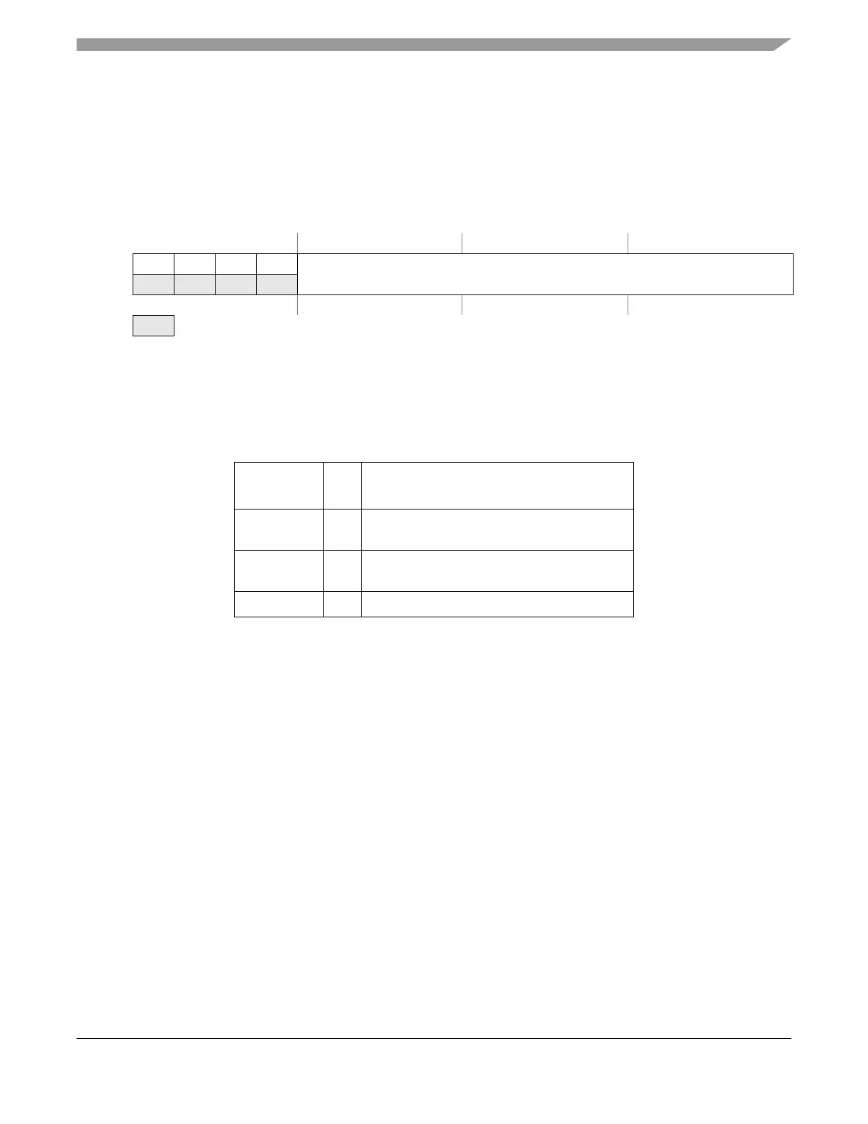
Module Base +
0x0010 = ATDDR0, 0x0012 = ATDDR1, 0x0014 = ATDDR2, 0x0016 = ATDDR3
0x0018 = ATDDR4, 0x001A = ATDDR5, 0x001C = ATDDR6, 0x001E = ATDDR7
0x0020 = ATDDR8, 0x0022 = ATDDR9, 0x0024 = ATDDR10, 0x0026 = ATDDR11
0x0028 = ATDDR12, 0x002A = ATDDR13, 0x002C = ATDDR14, 0x002E = ATDDR15
15 14 13 12 11 10 9 8 7 6 5 4 3 2 1 0
R 0 000
Result-Bit[11:0]
W
Reset0000000000000000
= Unimplemented or Reserved
Figure 16-15. Right justified ATD conversion result register (ATDDRn)
Table 16-22. Conversion result mapping to ATDDRn
A/D
resolution
DJM conversion result mapping to
ATDDRn
8-bit data 1 Result-Bit[7:0] = result,
Result-Bit[11:8]=0000
10-bit data 1 Result-Bit[9:0] = result,
Result-Bit[11:10]=00
12-bit data 1 Result-Bit[11:0] = result

 Loading...


