Serial Peripheral Interface (S12SPIV5)
MC9S12G Family Reference Manual Rev.1.27
708 NXP Semiconductors
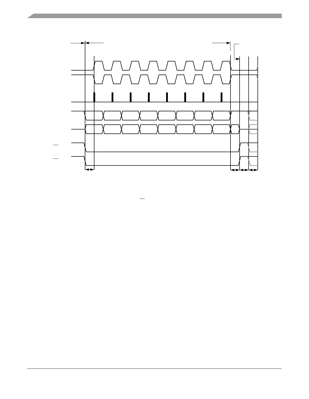
Figure 21-12. SPI Clock Format 0 (CPHA = 0), with 8-bit Transfer Width selected (XFRW = 0)
t
L
Begin End
SCK (CPOL = 0)
SAMPLE I
CHANGE O
SEL SS
(O)
Transfer
SCK (CPOL = 1)
MSB first (LSBFE = 0):
LSB first (LSBFE = 1):
MSB
LSB
LSB
MSB
Bit 5
Bit 2
Bit 6
Bit 1
Bit 4
Bit 3
Bit 3
Bit 4
Bit 2
Bit 5
Bit 1
Bit 6
CHANGE O
SEL SS
(I)
MOSI pin
MISO pin
Master only
MOSI/MISO
t
T
If next transfer begins here
for t
T
, t
l
, t
L
Minimum 1/2 SCK
t
I
t
L
t
L
= Minimum leading time before the first SCK edge
t
T
= Minimum trailing time after the last SCK edge
t
I
= Minimum idling time between transfers (minimum SS high time)
t
L
, t
T
, and t
I
are guaranteed for the master mode and required for the slave mode.
1 234 56 78910111213141516
SCK Edge Number
End of Idle State Begin of Idle State

 Loading...


