32 KByte Flash Module (S12FTMRG32K1V1)
MC9S12G Family Reference Manual Rev.1.27
NXP Semiconductors 825
The security function in the Flash module is described in Section 25.5.
25.3.2.3 Flash CCOB Index Register (FCCOBIX)
The FCCOBIX register is used to index the FCCOB register for Flash memory operations.
CCOBIX bits are readable and writable while remaining bits read 0 and are not writable.
25.3.2.4 Flash Reserved0 Register (FRSV0)
This Flash register is reserved for factory testing.
All bits in the FRSV0 register read 0 and are not writable.
Table 25-11. Flash Security States
SEC[1:0] Status of Security
00 SECURED
01 SECURED
1
1
Preferred SEC state to set MCU to secured state.
10 UNSECURED
11 SECURED
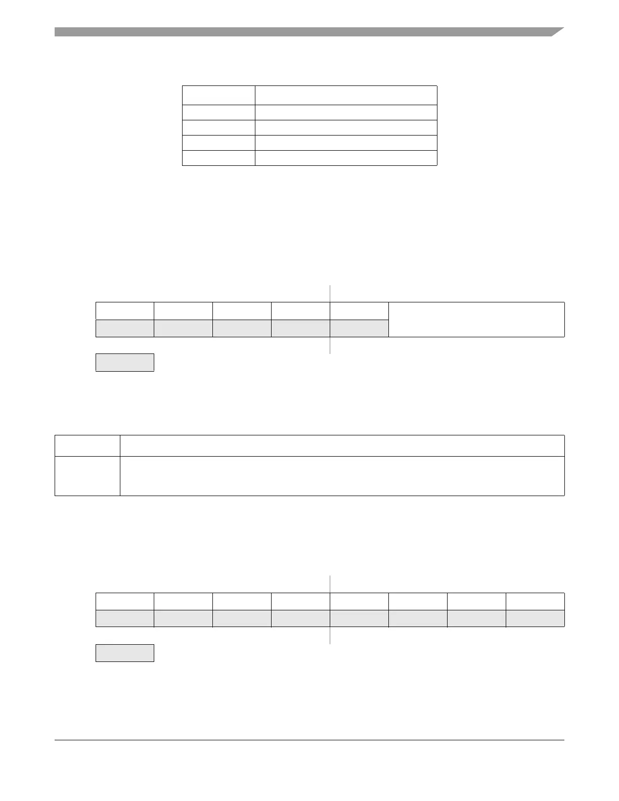
Offset Module Base + 0x0002
76543210
R00000
CCOBIX[2:0]
W
Reset00000000
= Unimplemented or Reserved
Figure 25-7. FCCOB Index Register (FCCOBIX)
Table 25-12. FCCOBIX Field Descriptions
Field Description
2–0
CCOBIX[1:0]
Common Command Register Index— The CCOBIX bits are used to select which word of the FCCOB register
array is being read or written to. See 25.3.2.11 Flash Common Command Object Register (FCCOB),” for more
details.
Offset Module Base + 0x000C
76543210
R00000000
W
Reset00000000
= Unimplemented or Reserved
Figure 25-8. Flash Reserved0 Register (FRSV0)

 Loading...


