32 KByte Flash Module (S12FTMRG32K1V1)
MC9S12G Family Reference Manual Rev.1.27
NXP Semiconductors 831
All possible P-Flash protection scenarios are shown in Figure 25-14 . Although the protection scheme is
loaded from the Flash memory at global address 0x3_FF0C during the reset sequence, it can be changed
by the user. The P-Flash protection scheme can be used by applications requiring reprogramming in single
chip mode while providing as much protection as possible if reprogramming is not required.
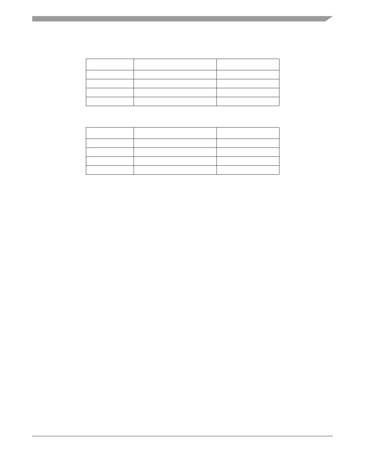
Table 25-19. P-Flash Protection Higher Address Range
FPHS[1:0] Global Address Range Protected Size
00 0x3_F800–0x3_FFFF 2 Kbytes
01 0x3_F000–0x3_FFFF 4 Kbytes
10 0x3_E000–0x3_FFFF 8 Kbytes
11 0x3_C000–0x3_FFFF 16 Kbytes
Table 25-20. P-Flash Protection Lower Address Range
FPLS[1:0] Global Address Range Protected Size
00 0x3_8000–0x3_83FF 1 Kbyte
01 0x3_8000–0x3_87FF 2 Kbytes
10 0x3_8000–0x3_8FFF 4 Kbytes
11 0x3_8000–0x3_9FFF 8 Kbytes

 Loading...


