48 KByte Flash Module (S12FTMRG48K1V1)
MC9S12G Family Reference Manual Rev.1.27
NXP Semiconductors 889
26.3.2.12 Flash Reserved1 Register (FRSV1)
This Flash register is reserved for factory testing.
All bits in the FRSV1 register read 0 and are not writable.
26.3.2.13 Flash Reserved2 Register (FRSV2)
This Flash register is reserved for factory testing.
All bits in the FRSV2 register read 0 and are not writable.
26.3.2.14 Flash Reserved3 Register (FRSV3)
This Flash register is reserved for factory testing.
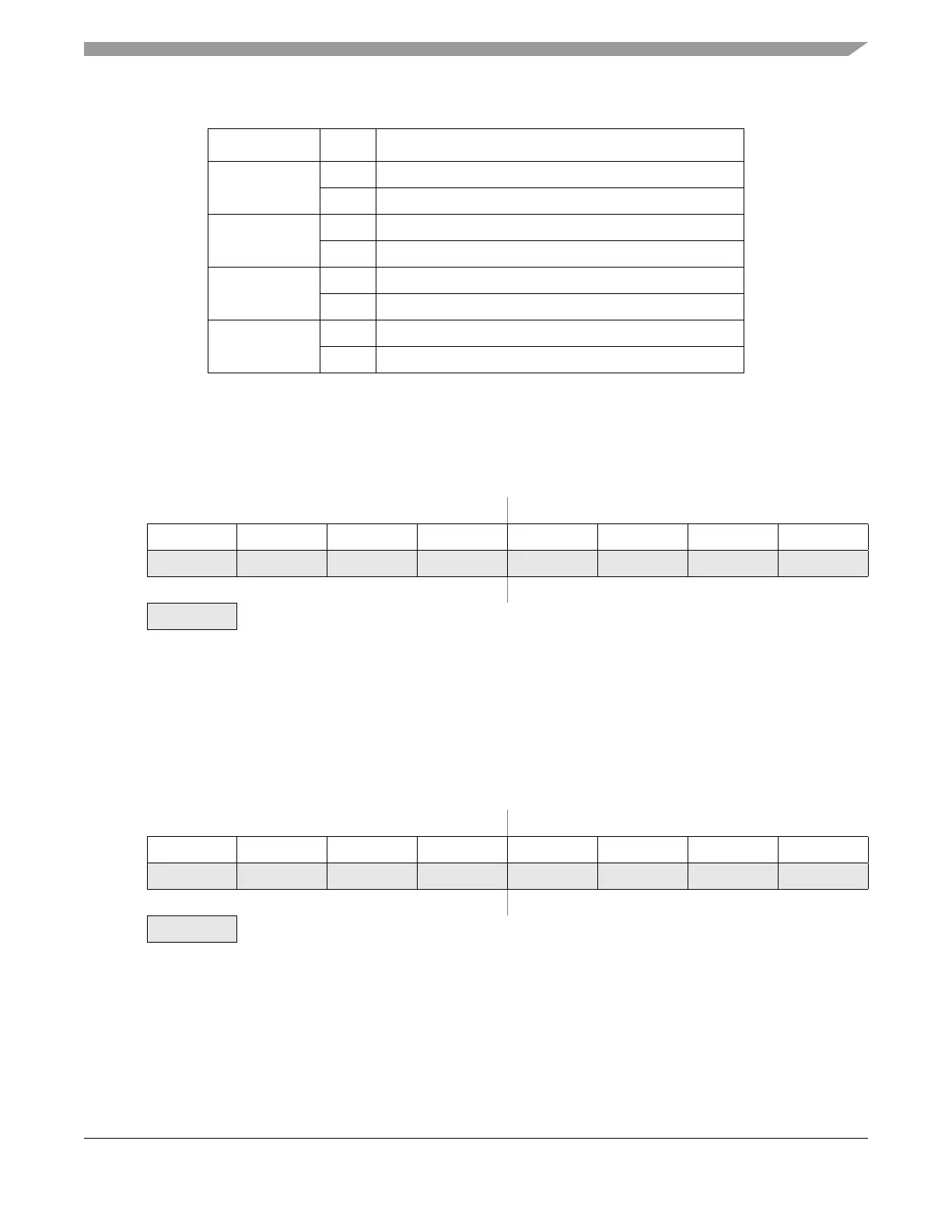
010
HI Data 0 [15:8]
LO Data 0 [7:0]
011
HI Data 1 [15:8]
LO Data 1 [7:0]
100
HI Data 2 [15:8]
LO Data 2 [7:0]
101
HI Data 3 [15:8]
LO Data 3 [7:0]
Offset Module Base + 0x000C
76543210
R00000000
W
Reset00000000
= Unimplemented or Reserved
Figure 26-18. Flash Reserved1 Register (FRSV1)
Offset Module Base + 0x000D
76543210
R00000000
W
Reset00000000
= Unimplemented or Reserved
Figure 26-19. Flash Reserved2 Register (FRSV2)
Table 26-24. FCCOB - NVM Command Mode (Typical Usage)
CCOBIX[2:0] Byte FCCOB Parameter Fields (NVM Command Mode)

 Loading...


