RL78/G15 CHAPTER 13 SERIAL INTERFACE IICA
R01UH0959EJ0110 Rev.1.10 Page 506 of 765
Mar 7, 2023
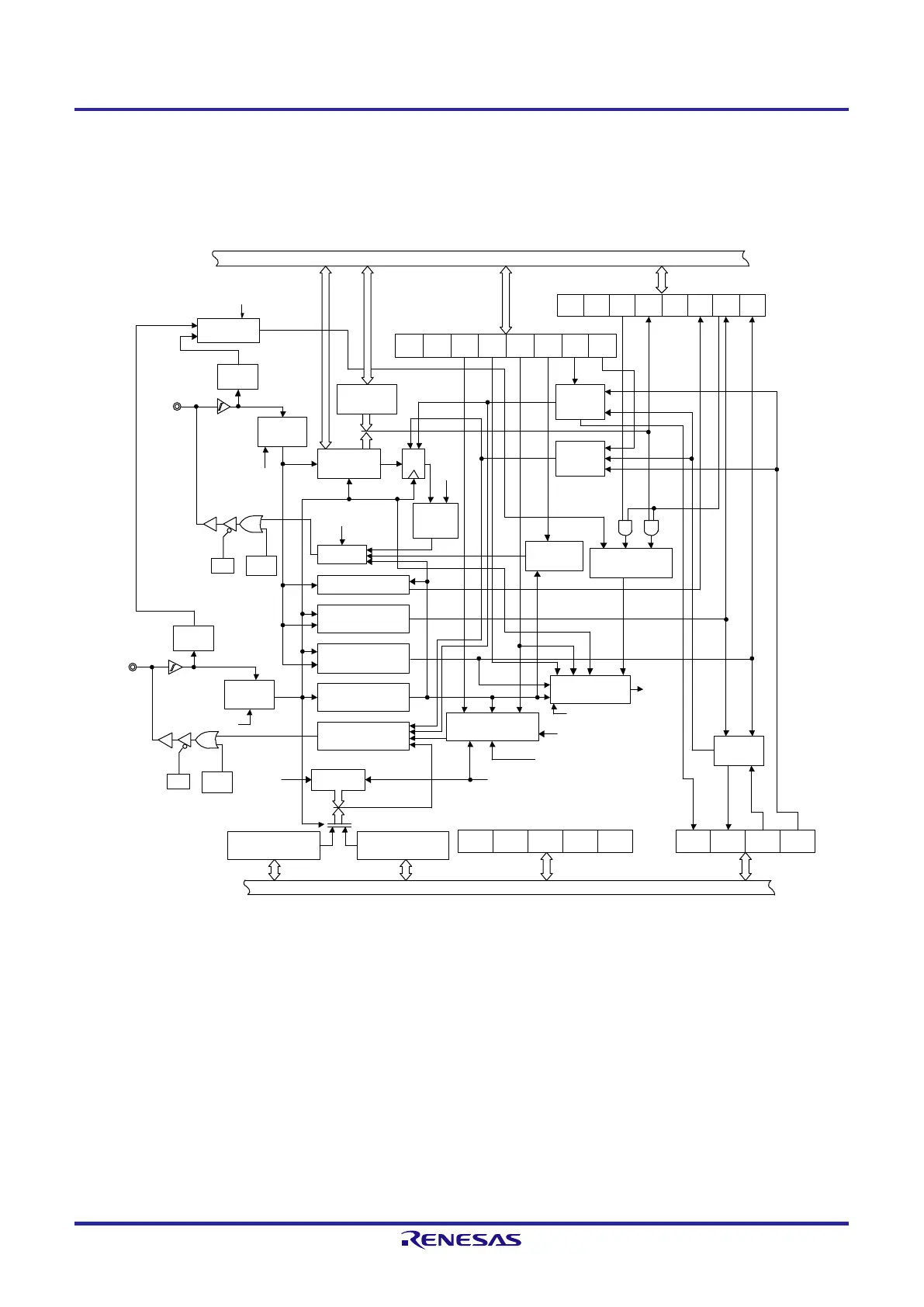
Figure 13-1 shows a block diagram of serial interface IICA.
Figure 13-1. Block Diagram of Serial Interface IICA
Slave address
register 0
(SVA0)
ACK generator
Data hold
time
correction
circuit
IICA shift
register 0
(IICA0)
Stop condition detector
IICE0
Internal bus
Serial clock counter
Interrupt request
signal generator
Serial clock controller
Counter
Clock stretch controller
MSTS0
Wakeup controller
Noise
eliminator
ACK detector
Filter
Filter
STOP mode
controller
Bus state
detector
Match
signal
Match signal
SO latch
WUP0
D Q
Set
Clear
IICWL0
TRC0
DFC0
DFC0
SDAA0/
P07
SCLA0/
P06
Start
condition
generator
Stop
condition
generator
Output
control
IICA low-level width
setting register 0
(IICWL0)
INTIICA0
IICCTL00.STT0, SPT0
IICS0.MSTS0, EXC0, COI0
IICS0.MSTS0, EXC0, COI0
f
CLK
Start condition detector
Internal bus
STCF0
WUP0
PM07
Output
latch
(P07)
PM06
Output
latch
(P06)
IICA high-level width
setting register 0
(IICWH0)
IICA control register 01
(IICCTL01)
IICA shift register 0 (IICA0)
N-ch open-drain
output
IICA status register 0
(IICS0)
IICA control register 00
(IICCTL00)
LREL0
WREL0
SPIE0
WTIM0
ACKE0
STT0
SPT0
ALD0
EXC0
COI0
TRC0
ACKD0
STD0
SPD0
CLD0
DAD0
SMC0
DFC0
IICBSY0
STCEN0
IICRSV0
IICA flag register 0
(IICF0)
Noise
eliminator
N-ch open-drain
output
Remark The IICA pins in this figure are when PIOR14 = 0 for 16- and 20-pin products.
 Loading...


