RL78/G15 CHAPTER 13 SERIAL INTERFACE IICA
R01UH0959EJ0110 Rev.1.10 Page 520 of 765
Mar 7, 2023
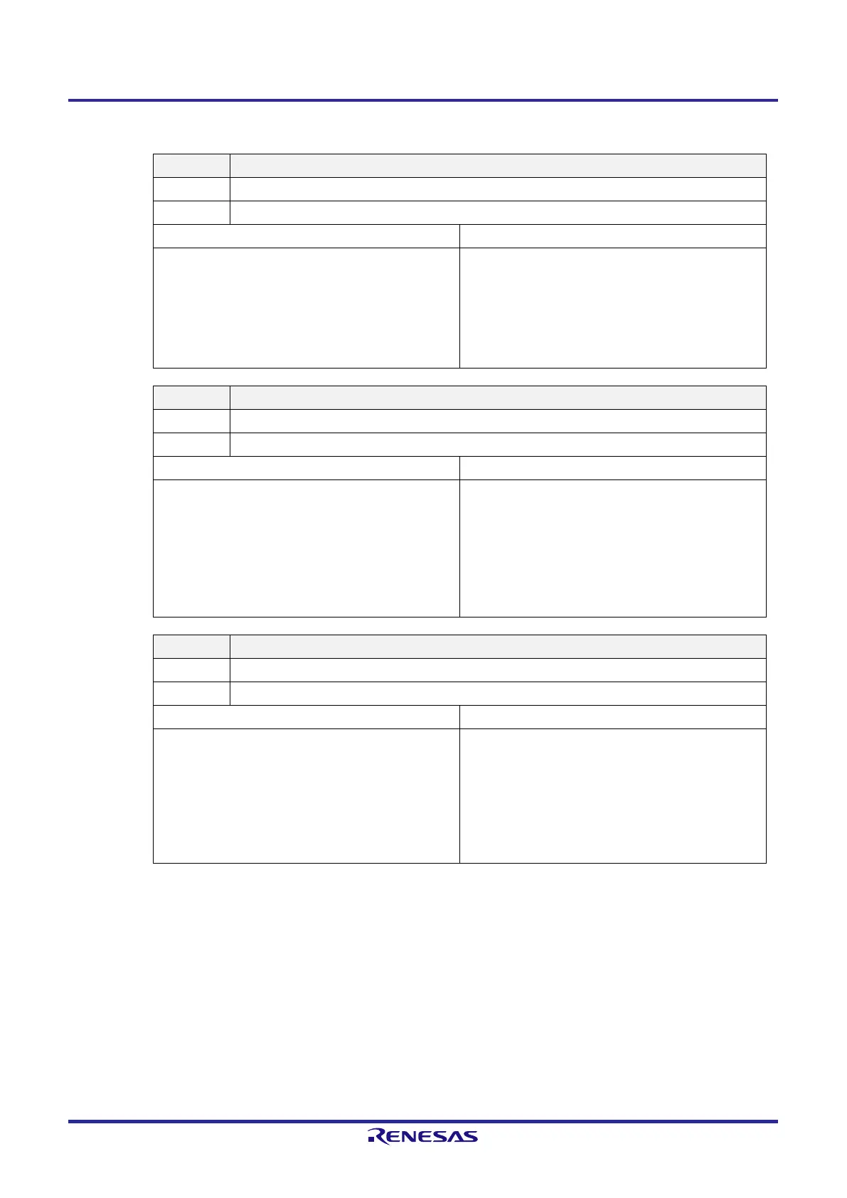
Figure 13-7. Format of IICA Status Register 0 (IICS0) (3/3)
ACKD0 Acknowledge (ACK) detection
0 Acknowledge was not detected.
1 Acknowledge was detected.
Condition for clearing (ACKD0 = 0) Condition for setting (ACKD0 = 1)
●
When a stop condition is detected
●
At the rising edge of the first clock of the next byte
●
Cleared by LREL0 = 1 (exit from communications)
●
When the IICE0 bit changes from 1 to 0 (operation
stop)
●
Reset
●
When the SDAA0 line is at the low level at the rising
edge of the 9th clock of the SCLA0 line
STD0 Start condition detection
0 A start condition was not detected.
1 A start condition was detected. This indicates that the address transfer period is in effect.
Condition for clearing (STD0 = 0) Condition for setting (STD0 = 1)
●
When a stop condition is detected
●
At the rising edge of the first clock of the next byte
following address transfer
●
Cleared by LREL0 = 1 (exit from communications)
●
When the IICE0 bit changes from 1 to 0 (operation
stop)
●
Reset
●
When a start condition is detected
SPD0 Stop condition detection
0 A stop condition was not detected.
1 A stop condition was detected. Communication by the master is terminated and the bus is released.
Condition for clearing (SPD0 = 0) Condition for setting (SPD0 = 1)
●
At the rising edge of the first clock of the address
transfer byte following setting of this bit and detection of
a start condition
●
When the WUP0 bit changes from 1 to 0
●
When the IICE0 bit changes from 1 to 0 (operation
stop)
●
Reset
●
When a stop condition is detected
Note 1. The ALD0 bit is also cleared when a 1-bit memory manipulation instruction is executed for another bit in the
IICS0 register. Therefore, when using the ALD0 bit, read the data of this bit before the data of the other bits.
Note 2. While bit 3 (TRC0) of IICA status register 0 (IICS0) is 1 (transmission state), if bit 5 (WREL0) of IICA control
register 00 (IICCTL00) is set to 1 at the 9th clock to release clock stretching, the TRC0 bit is cleared
(reception state) and the SDAA0 line is set to the high impedance state. Release clock stretching while the
TRC0 bit is 1 (transmission state) by writing to IICA shift register 0.
Remark LREL0: Bit 6 of IICA control register 00 (IICCTL00)
IICE0: Bit 7 of IICA control register 00 (IICCTL00)
 Loading...


