RL78/G15 CHAPTER 24 ELECTRICAL SPECIFICATIONS (T
A
= −40 to +105°C, TA = −40 to +125°C)
R01UH0959EJ0110 Rev.1.10 Page 735 of 765
Mar 7, 2023
Remark The characteristics of functions multiplexed on a given pin are the same as those for the port pin unless
otherwise specified.
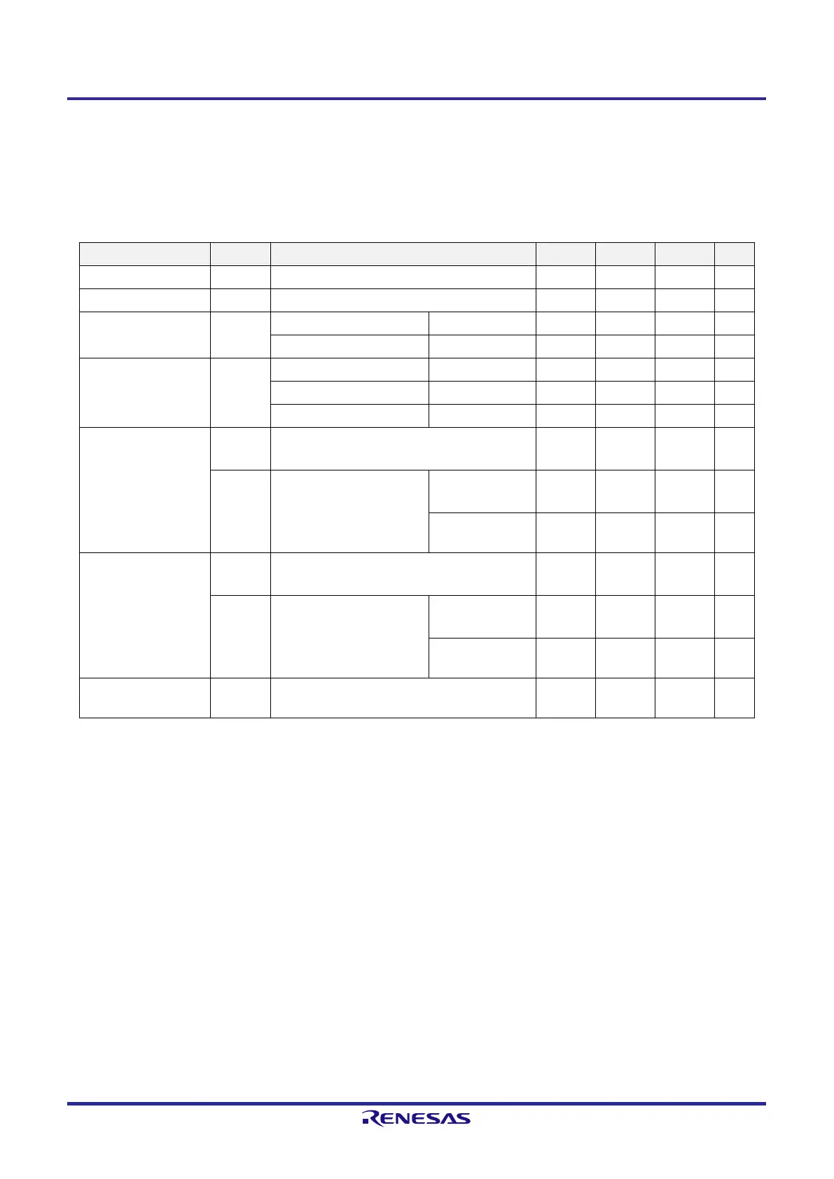
[T
A
= −40 to +105°C: G products, T
A
= −40 to +125°C: M products, 2.4 V ≤ V
DD
≤ 5.5 V, V
SS
= 0 V]
(2/2)
Item Symbol Condition MIN. TYP. MAX. Unit
Input voltage, high V
IH1
0.8 V
DD
V
DD
V
Input voltage, low V
IL1
0 0.2 V
DD
V
Output voltage, high
Note 1
V
OH1
4.0 V ≤ V
DD
≤ 5.5 V I
OH
= −3.0 mA V
DD
− 0.7 V
2.4 V ≤ V
DD
≤ 5.5 V I
OH
= −1.0 mA V
DD
− 0.5 V
Output voltage, low
Note 2
V
OL1
4.0 V ≤ V
DD
≤ 5.5 V I
OL
= 8.5 mA 0.7 V
2.7 V ≤ V
DD
≤ 5.5 V I
OL
= 1.5 mA 0.5 V
2.4 V ≤ V
DD
≤ 5.5 V I
OL
= 0.6 mA 0.4 V
Input leakage current,
high
I
LIH1
P00 to P07, P20 to P23, P40, P41, P125, P137
V
I
=V
DD
1 µA
I
LIH2
P121, P122 (X1, X2, EXCLK)
V
I
= V
DD
In input port or
external clock input
1 µA
In resonator
connection
10 µA
Input leakage current,
low
I
LIL1
P00 to P07, P20 to P23, P40, P41, P125, P137
V
I
= V
SS
−1 µA
I
LIL2
P121, P122 (X1, X2, EXCLK)
V
I
= V
SS
In input port or
external clock input
−1 µA
In resonator
connection
−10 µA
On-chip pull-up
resistance
R
U
V
I
= V
SS
10 20 100 kΩ
Note 1. The value under the condition which satisfies the high-level output current (I
OH1
).
Note 2. The value under the condition which satisfies the low-level output current (I
OL1
).
Caution The maximum value of V
IH
of P00, P01, P03 to P07, P22, and P41 is V
DD
even in N-ch open-drain mode.
These pins do not output high level in N-ch open-drain mode.
Remark The characteristics of functions multiplexed on a given pin are the same as those for the port pin unless
otherwise specified.
 Loading...


