RL78/G15 CHAPTER 3 CPU ARCHITECTURE
R01UH0959EJ0110 Rev.1.10 Page 93 of 765
Mar 7, 2023
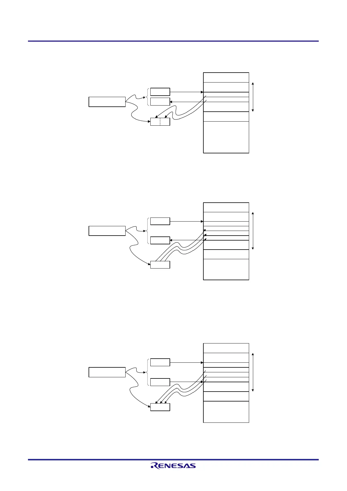
Figure 3-33. Example of POP
Instruction code
OP-code
Memory
F0000H
• Stack addressing is specified <1>.
• The contents of addresses SP and SP + 1 are stored in the
lower-order and higher-order bytes of the pair of registers
indicated by rp <2>, respectively.
• The value of SP <3> is increased by two (if rp is the program
status word (PSW), the content of address SP + 1 is stored
in the PSW).
(SP + 1)
SP + 1
SP
POP
<1>
rp
<2>
SP
(SP)
Stack
area
SP
<3>
rp
<1>
<2>
SP + 2
Figure 3-34. Example of CALL, CALLT
Instruction code
OP-code
Memory
F
0000H
• Stack addressing is specified <1>. The value of the program
counter (
PC) changes to indicate the address of the instruction
following the CALL instruction.
• The values of PC bits 19 to 16, 15 to 8, and 7 to 0 are stored in
addresses SP
– 2
, SP -
3, and SP
– 4,
respectively <2>.
• The value of the SP <3> is decreased by 4.
PC19 to PC16
SP
– 1
SP – 2
SP –
3
SP
– 4
CALL
<1
>
SP
PC
15 to PC8
Stack
area
SP
<3>
PC
<1
>
PC
7 to PC0
<2
>
Figure 3-35. Example of RET
Instruction code
OP-code
Memory
F0000H
•
Stack addressing is specified <1>.
• The contents of addresses SP, SP + 1, and SP + 2 are stored in
PC bits 7 to 0, 15 to 8, and 19 to 16, respectively <2>.
• The value of SP <3> is increased by four.
(SP + 2)
SP + 3
SP + 2
SP + 1
SP
RET
<1>
SP
(SP + 1)
Stack
area
SP
<3>
PC
<1>
(SP)
(SP + 3)
<2>
SP + 4
 Loading...


