5–38 Chapter 5: Clock Networks and PLLs in Cyclone IV Devices
PLL Reconfiguration
Cyclone IV Device Handbook, October 2012 Altera Corporation
Volume 1
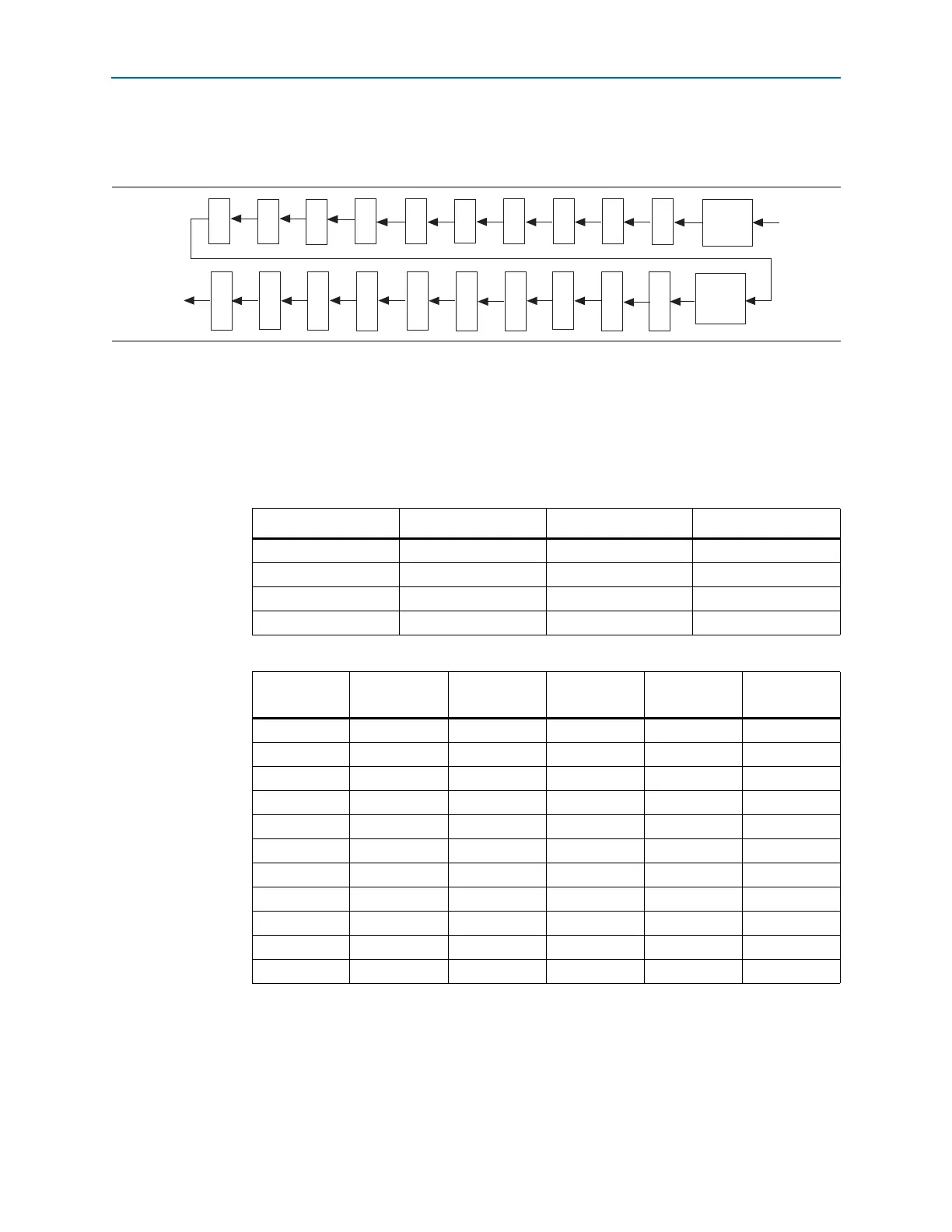
Figure 5–25 shows the scan chain bit order sequence for one PLL post-scale counter in
PLLs of Cyclone IV devices.
Charge Pump and Loop Filter
You can reconfigure the charge pump and loop filter settings to update the PLL
bandwidth in real time. Table 5–8 through Table 5–10 list the possible settings for
charge pump current (
I
CP
), loop filter resistor (R), and capacitor (C) values for PLLs of
Cyclone IV devices.
Figure 5–25. Scan Chain Bit Order
DATAIN
rbypass
HB
7
HB
6
HB
5
HB
4
HB
3
HB
2
HB
1
HB
0
rselodd
LB
7
LB
6
LB
5
LB
4
LB
3
LB
2
LB
1
LB
0
DATAOUT
HB
9
HB
8
LB
9
LB
8
Table 5–8. Charge Pump Bit Control
CP[2] CP[1] CP[0] Setting (Decimal)
0000
1001
1103
1117
Table 5–9. Loop Filter Resistor Value Control
LFR[4] LFR[3] LFR[2] LFR[1] LFR[0]
Setting
(Decimal)
000000
000113
001004
010008
1000016
1001119
1010020
1100024
1101127
1110028
1111030