Chapter 2: Cyclone IV Reset Control and Power Down 2–17
Transceiver Reset Sequences
September 2014 Altera Corporation Cyclone IV Device Handbook,
Volume 2
PCIe Functional Mode
You can configure PCIe functional mode with or without the receiver clock rate
compensation FIFO in the Cyclone IV GX device. The reset sequence remains the
same whether or not you use the receiver clock rate compensation FIFO.
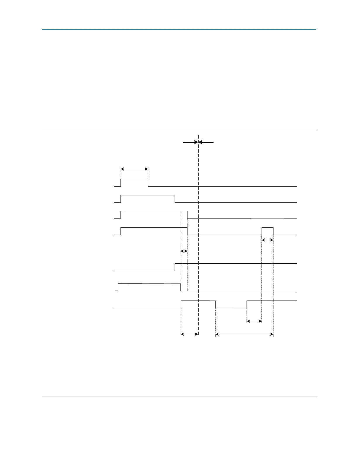
PCIe Reset Sequence
The PCIe protocol consists of an initialization/compliance phase and a normal
operation phase. The reset sequences for these two phases are described based on the
timing diagram in Figure 2–10.
Figure 2–10. Reset Sequence of PCIe Functional Mode
(1)
,
(2)
Notes to Figure 2–10:
(1) This timing diagram is drawn based on the PCIe Gen 1 ×1 mode.
(2) For bonded PCIe Gen 1 ×2 and ×4 modes, there will be additional
rx_freqlocked[n]
signal. n=number of channels.
(3) For t
LTD_Manual
duration, refer to the Cyclone IV Device Datasheet chapter.
(4) For t
LTD_Auto
duration, refer to the Cyclone IV Device Datasheet chapter.
(5) The
busy
signal is asserted and deasserted only during initial power up when offset cancellation occurs. In subsequent reset sequences, the
busy
signal is asserted and deasserted only if there is a read or write operation to the ALTGX_RECONFIG megafunction.
12
3
4
6
7
8
Ignore receive data
910
11 12
Two parallel
clock cycles
> two parallel
clock cycles
_
5
1 μs
Reset / Power Down Signals
Output Status Signals
busy (5)
pll_areset
tx_digitalreset
rx_analogreset
rx_digitalreset
rx_freqlocked
pll_locked
Initialization / Compliance Phase
Normal Operation Phase
t
LTD_Manual
(3)
t
LT D _ Au t o
(4)