Chapter 1: Cyclone IV Transceivers Architecture 1–27
Transceiver Clocking Architecture
February 2015 Altera Corporation Cyclone IV Device Handbook,
Volume 2
Input Reference Clocking
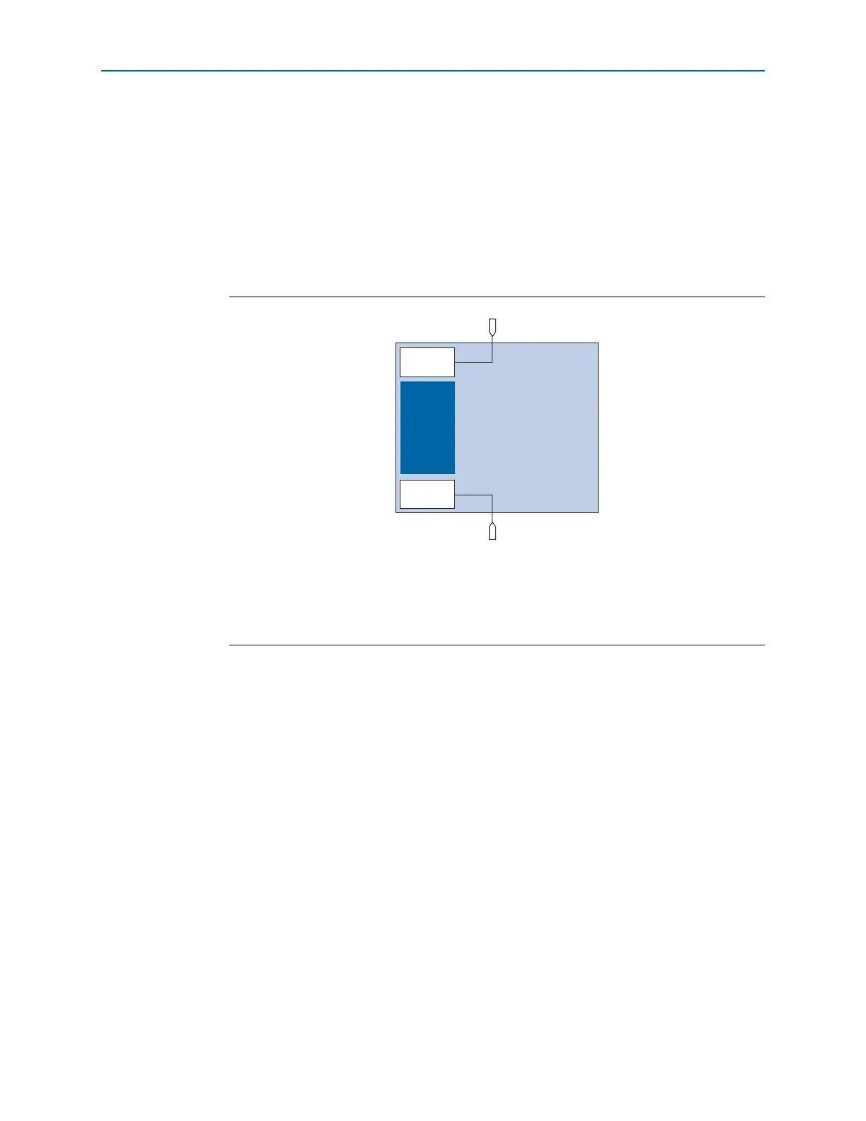
When used for transceiver, the left PLLs synthesize the input reference clock to
generate the required clocks for the transceiver channels. Figure 1–25 and Figure 1–26
show the sources of input reference clocks for PLLs used in the transceiver operation.
1 Clock output from PLLs in the FPGA core cannot feed into PLLs used by the
transceiver as input reference clock.
Figure 1–25. PLL Input Reference Clocks in Transceiver Operation for F324 and Smaller
Packages
(1)
,
(2)
Notes to Figure 1–25:
(1) The
REFCLK0
and
REFCLK1
pins are dual-purpose
CLK
,
REFCLK
, or
DIFFCLK
pins that reside in banks 3A and 8A
respectively.
(2) Using any clock input pins other than the designated
REFCLK
pins as shown here to drive the MPLLs may have
reduced jitter performance.
Transceiver
Block
GXBL0
MPLL_2
REFCLK1
REFCLK0
MPLL_1