Chapter 2: Logic Elements and Logic Array Blocks in Cyclone IV Devices 2–7
Document Revision History
November 2009 Altera Corporation Cyclone IV Device Handbook,
Volume 1
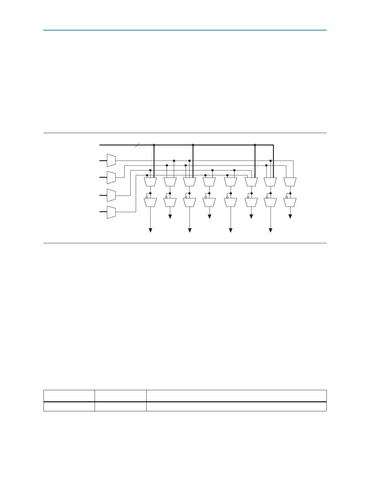
Each LAB can use two clocks and two clock enable signals. The clock and clock enable
signals of each LAB are linked. For example, any LE in a particular LAB using the
labclk1
signal also uses the
labclkena1
. If the LAB uses both the rising and falling
edges of a clock, it also uses both LAB-wide clock signals. Deasserting the clock
enable signal turns off the LAB-wide clock.
The LAB row clocks
[5..0]
and LAB local interconnect generate the LAB-wide
control signals. The MultiTrack interconnect inherent low skew allows clock and
control signal distribution in addition to data distribution.
Figure 2–6 shows the LAB control signal generation circuit.
LAB-wide signals control the logic for the clear signal of the register. The LE directly
supports an asynchronous clear function. Each LAB supports up to two asynchronous
clear signals (
labclr1
and
labclr2
).
A LAB-wide asynchronous load signal to control the logic for the preset signal of the
register is not available. The register preset is achieved with a NOT gate push-back
technique. Cyclone IV devices only support either a preset or asynchronous clear
signal.
In addition to the clear port, Cyclone IV devices provide a chip-wide reset pin
(
DEV_CLRn
) that resets all registers in the device. An option set before compilation in
the Quartus II software controls this pin. This chip-wide reset overrides all other
control signals.
Document Revision History
Tab le 2 –1 shows the revision history for this chapter.
Figure 2–6. Cyclone IV Device LAB-Wide Control Signals
labclkena1
labclk2labclk1
labclkena2
labclr1
Dedicated
LAB Row
Clocks
Local
Interconnect
Local
Interconnect
Local
Interconnect
Local
Interconnect
syncload
synclr
labclr2
6
Table 2–1. Document Revision History
Date Version Changes
November 2009 1.0 Initial release.