Chapter 5: Clock Networks and PLLs in Cyclone IV Devices 5–25
Clock Feedback Modes
October 2012 Altera Corporation Cyclone IV Device Handbook,
Volume 1
Figure 5–14 shows a waveform example of the phase relationship of the PLL clocks in
this mode.
Zero Delay Buffer Mode
In zero delay buffer (ZDB) mode, the external clock output pin is phase-aligned with
the clock input pin for zero delay through the device. When using this mode, use the
same I/O standard on the input clock and output clocks to guarantee clock alignment
at the input and output pins.
Figure 5–15 shows an example waveform of the phase relationship of the PLL clocks
in ZDB mode.
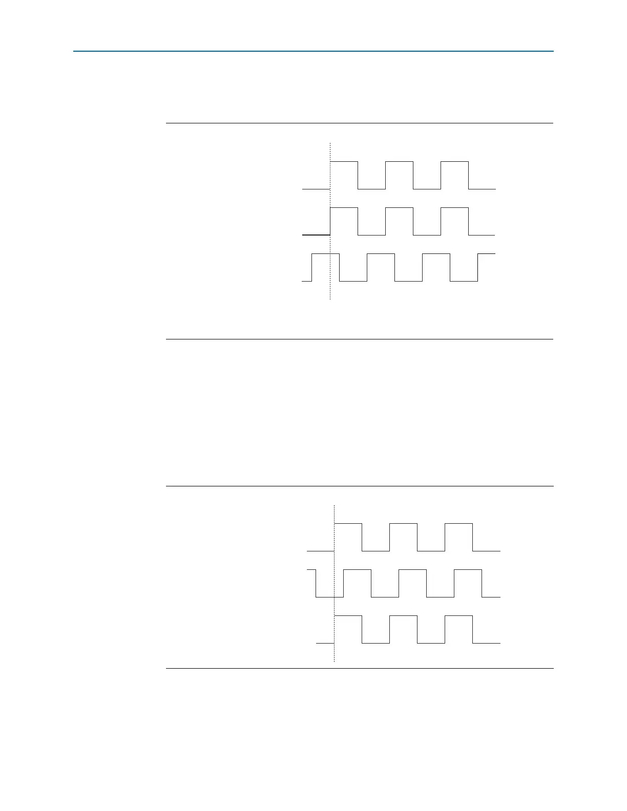
Figure 5–14. Phase Relationship Between PLL Clocks in Normal Mode
Note to Figure 5–14:
(1) The external clock output can lead or lag the PLL internal clock signals.
PLL Reference
Clock at the Input pin
PLL Clock at the
Register Clock Port
External PLL Clock
Outputs
(1)
Phase Aligned
Figure 5–15. Phase Relationship Between PLL Clocks in ZDB Mode
PLL Reference Clock
at the Input Pin
PLL Clock
at the Register Clock Port
External PLL Clock Output
at the Output Pin
Phase Aligned