5–18 Chapter 5: Clock Networks and PLLs in Cyclone IV Devices
PLLs in Cyclone IV Devices
Cyclone IV Device Handbook, October 2012 Altera Corporation
Volume 1
PLLs in Cyclone IV Devices
Cyclone IV GX devices offer two variations of PLLs: general purpose PLLs and
multipurpose PLLs. Cyclone IV E devices only have the general purpose PLLs.
The general purpose PLLs are used for general-purpose applications in the FPGA
fabric and periphery such as external memory interfaces. The multipurpose PLLs are
used for clocking the transceiver blocks. When the multipurpose PLLs are not used
for transceiver clocking, they can be used for general-purpose clocking.
f For more details about the multipurpose PLLs used for transceiver clocking, refer to
the Cyclone IV Transceivers chapter.
Cyclone IV GX devices contain up to eight general purpose PLLs and multipurpose
PLLs while Cyclone IV E devices have up to four general purpose PLLs that provide
robust clock management and synthesis for device clock management, external
system clock management, and high-speed I/O interfaces.
f For more information about the number of general purpose PLLs and multipurpose
PLLs in each device density, refer to the Cyclone IV Device Family Overview chapter.
1 The general I/O pins cannot drive the PLL clock input pins.
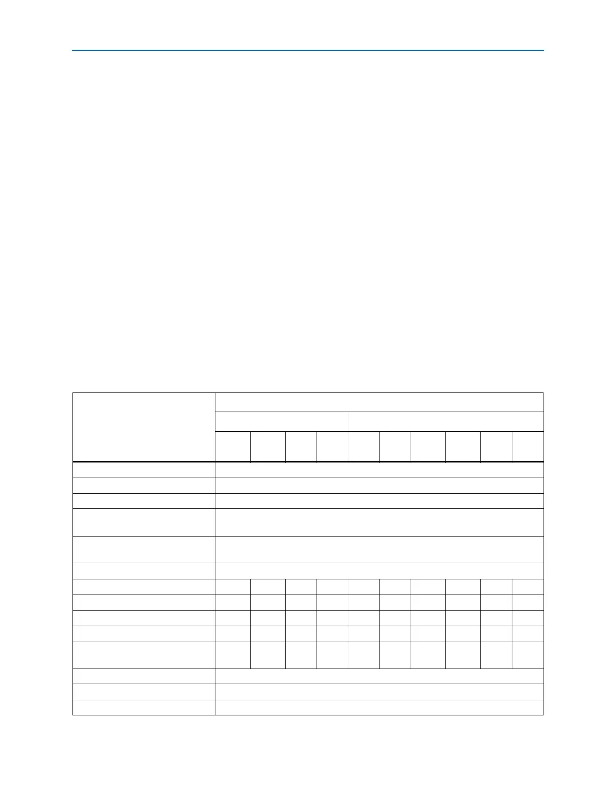
Tab le 5 –5 lists the features available in Cyclone IV GX PLLs.
Table 5–5. Cyclone IV GX PLL Features (Part 1 of 2)
Features
Availability
General Purpose PLLs Multipurpose PLLs
PLL_1
(1), (10)
PLL_2
(1), (10)
PLL_
3
(2)
PLL_
4
(3)
PLL_1
(4)
PLL_2
(4)
PLL_5
(1), (10)
PLL_6
(1), (10)
PLL_7
(1)
PLL_8
(1)
C (output counters) 5
M, N, C counter sizes 1 to 512
(5)
Dedicated clock outputs 1 single-ended or 1 differential pair
Clock input pins
12 single-ended or 6 differential pairs
(6)
and 4 differential pairs
(7)
Spread-spectrum input clock
tracking
v
(8)
PLL cascading Through GCLK
Source
-Synchronous Mode v vvvvvv ——v
No Compensation Mode v vvvvvv vvv
Normal Mode v vvvvvv ——v
Zero Delay Buffer Mode v vvvvvv ——v
Deterministic Latency
Compensation Mode
vv——vvv vvv
Phase shift resolution
(9)
Down to 96 ps increments
Programmable duty cycle v
Output counter cascading v