5–16 Chapter 5: Clock Networks and PLLs in Cyclone IV Devices
Clock Networks
Cyclone IV Device Handbook, October 2012 Altera Corporation
Volume 1
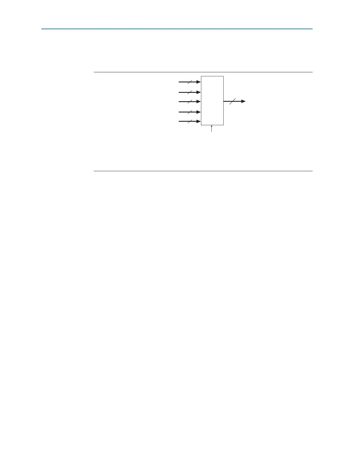
Figure 5–6 shows a simplified version of the five clock control blocks on each side of
the Cyclone IV E device periphery.
GCLK Network Power Down
You can disable a Cyclone IV device’s GCLK (power down) using both static and
dynamic approaches. In the static approach, configuration bits are set in the
configuration file generated by the Quartus II software, which automatically disables
unused GCLKs. The dynamic clock enable or disable feature allows internal logic to
control clock enable or disable the GCLKs in Cyclone IV devices.
When a clock network is disabled, all the logic fed by the clock network is in an
off-state, thereby reducing the overall power consumption of the device. This function
is independent of the PLL and is applied directly on the clock network, as shown in
Figure 5–1 on page 5–11.
You can set the input clock sources and the
clkena
signals for the GCLK multiplexers
through the Quartus II software using the ALTCLKCTRL megafunction.
f For more information, refer to the ALTCLKCTRL Megafunction User Guide.
clkena Signals
Cyclone IV devices support
clkena
signals at the GCLK network level. This allows
you to gate-off the clock even when a PLL is used. Upon re-enabling the output clock,
the PLL does not need a resynchronization or re-lock period because the circuit gates
off the clock at the clock network level. In addition, the PLL can remain locked
independent of the
clkena
signals because the loop-related counters are not affected.
Figure 5–6. Clock Control Blocks on Each Side of Cyclone IV E Device
(1)
Note to Figure 5–6:
(1) The left and right sides of the device have two
DPCLK
pins; the top and bottom of the device have four
DPCLK
pins.
5
GCLK
Clock Input Pins
3 or 4
DPCLK
Internal Logic
Clock
Control
Block
5
PLL Outputs
5
2 or 4
CDPCLK
2
Five Clock Control
Blocks on Each Side
of the Device