Chapter 1: Cyclone IV Transceivers Architecture 1–37
Transceiver Clocking Architecture
February 2015 Altera Corporation Cyclone IV Device Handbook,
Volume 2
Bonded Channel Configuration
In bonded channel configuration, the low-speed clock for the bonded channels share a
common bonded clock path that reduces clock skew between the bonded channels.
The phase compensation FIFOs in bonded channels share a set of pointers and control
logic that results in equal FIFO latency between the bonded channels. These features
collectively result in lower channel-to-channel skew when implementing
multi-channel serial interface in bonded channel configuration.
In a transceiver block, the high-speed clock for each bonded channels is distributed
independently from one of the two multipurpose PLLs directly adjacent to the block.
The low-speed clock for bonded channels is distributed from a common bonded clock
path that selects from one of the two multipurpose PLLs directly adjacent to the block.
Transceiver channels for devices in F484 and larger packages support additional
clocking flexibility for ×2 bonded channels. In these packages, the ×2 bonded channels
support high-speed and low-speed bonded clock distribution from PLLs beyond the
two multipurpose PLLs directly adjacent to the block. Table 1–10 lists the high- and
low-speed clock sources for the bonded channels.
1 When implementing ×2 bonded channel configuration in a transceiver block,
remaining channels 2 and 3 are available to implement other non-bonded channel
configuration.
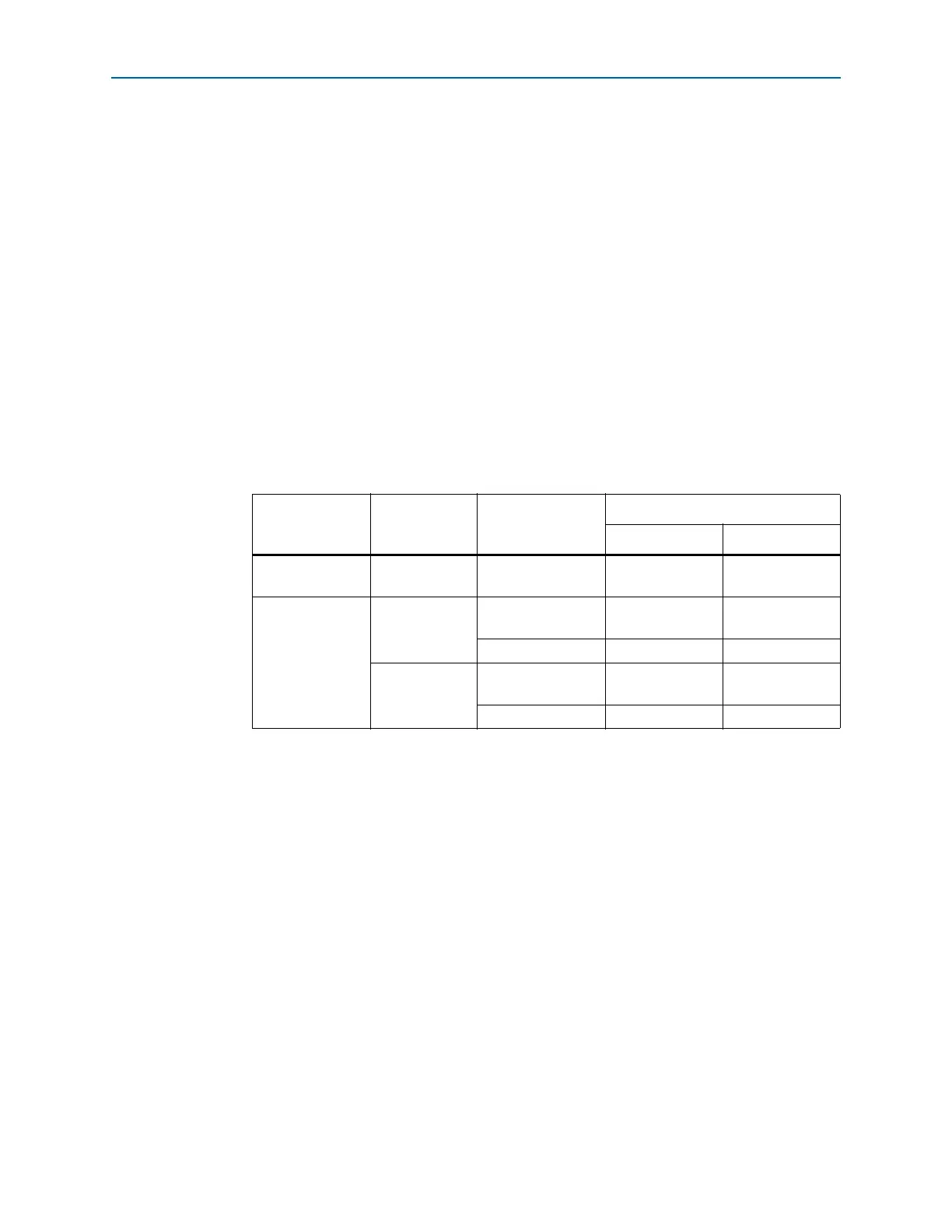
Table 1–10. High- and Low-Speed Clock Sources for Bonded Channels in Bonded Channel
Configuration
Package
Transceiver
Block
Bonded Channels
High- and Low-Speed Clocks Source
Option 1 Option 2
F324 and smaller
GXBL0
×2 in channels 0, 1
×4 in all channels
MPLL_1 MPLL_2
F484 and larger
GXBL0
×2 in channels 0, 1
MPLL_5/
GPLL_1
MPLL_6
×4 in all channels
MPLL_5 MPLL_6
GXBL1 (1)
×2 in channels 0, 1
MPLL_7/
MPLL_6
MPLL_8
×4 in all channels
MPLL_7 MPLL_8
Note to Table 1–10:
(1)
GXBL1
is not available for transceivers in F484 package.