Chapter 3: Cyclone IV Dynamic Reconfiguration 3–33
Dynamic Reconfiguration Modes
November 2011 Altera Corporation Cyclone IV Device Handbook,
Volume 2
Option 3: Use the Respective Channel Receiver Core Clocks
■ Enable this option if you want the individual channel’s
rx_clkout
signal to
provide the read clock to its respective Receive Phase Compensation FIFO.
■ This option is typically enabled when the channel is reconfigured from a Basic or
Protocol configuration with or without rate matching to another Basic or Protocol
configuration with or without rate matching.
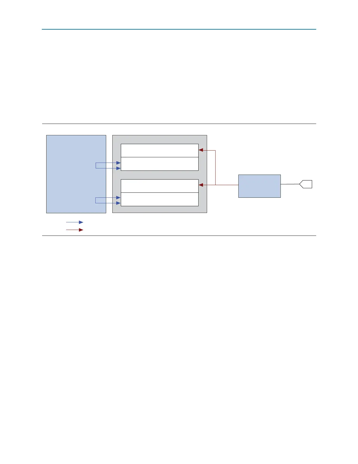
Figure 3–15 shows the respective
rx_clkout
of each channel clocking the respective
receiver channels of a transceiver block.
PLL Reconfiguration Mode
Cyclone IV GX device support the PLL reconfiguration support through the
ALTPLL_RECONFIG MegaWizard. You can use this mode to reconfigure the
multipurpose PLL or general purpose PLL used to clock the transceiver channel
without affecting the remaining blocks of the channel. When you reconfigure the
multipurpose PLL or general purpose PLL of a transceiver block to run at a different
data rate, all the transceiver channels listening to this
multipurpose PLL or general
purpose PLL
also get reconfigured to the new data rate. Channel settings are not
affected.
When you reconfigure the multipurpose PLL or general purpose PLL to support
a different data rate, you must ensure that the functional mode of the transceiver channel
supports the reconfigured data rate.
The PLL reconfiguration mode can be enabled by selecting the Enable PLL
Reconfiguration option in the ALTGX MegaWizard under Reconfiguration Setting
tab. For
multipurpose PLL or general purpose PLL reconfiguration, .mif files are
required to dynamically reconfigure the PLL setting in order to change the output
frequency of the transceiver PLL to support different data rates.
Figure 3–15. Option 3 for Receiver Core Clocking (Channel Reconfiguration Mode)
High-speed serial clock generated by the MPLL
FPGA Fabric Transceiver Block
rx_clkout[0]
rx_clkout[1]
RX1
RX0
TX0
TX1
MPLL
Low-speed parallel clock