6–28 Chapter 6: I/O Features in Cyclone IV Devices
High-Speed I/O Standards Support
Cyclone IV Device Handbook, March 2016 Altera Corporation
Volume 1
High-Speed I/O Standards Support
This section provides information about the high-speed I/O standards and the HSSI
input reference clock supported in Cyclone IV devices.
High Speed Serial Interface (HSSI) Input Reference Clock Support
Cyclone IV GX devices support the same I/O features for GPIOs with additional new
features where current I/O banks 3A and 8A consist of dual-purpose clock input pins
(
CLKIN
) and 3B and 8B consist of dedicated
CLKIN
that can be used to support the high-
speed transceiver input reference clock (
REFCLK
) features on top of the
general-purpose clock input function.
The EP4CGX15, EP4CGX22, and EP4CGX30 devices contain two pairs of
CLKIN/REFCLK
pins located in I/O banks 3A and 8A. I/O banks 3B and 8B are not
available in EP4CGX15, EP4CGX22, and EP4CGX30 devices. The EP4CGX50,
EP4CGX75, EP4CGX110, and EP4CGX150 devices have a total of four pairs of
CLKIN/REFCLK
pins located in I/O banks 3A, 3B, 8A, and 8B. I/O banks 3B and 8B can
also support single-ended clock inputs. For more information about the
CLKIN/REFCLK
pin location, refer to Figure 6–10 on page 6–18 and Figure 6–11 on page 6–19.
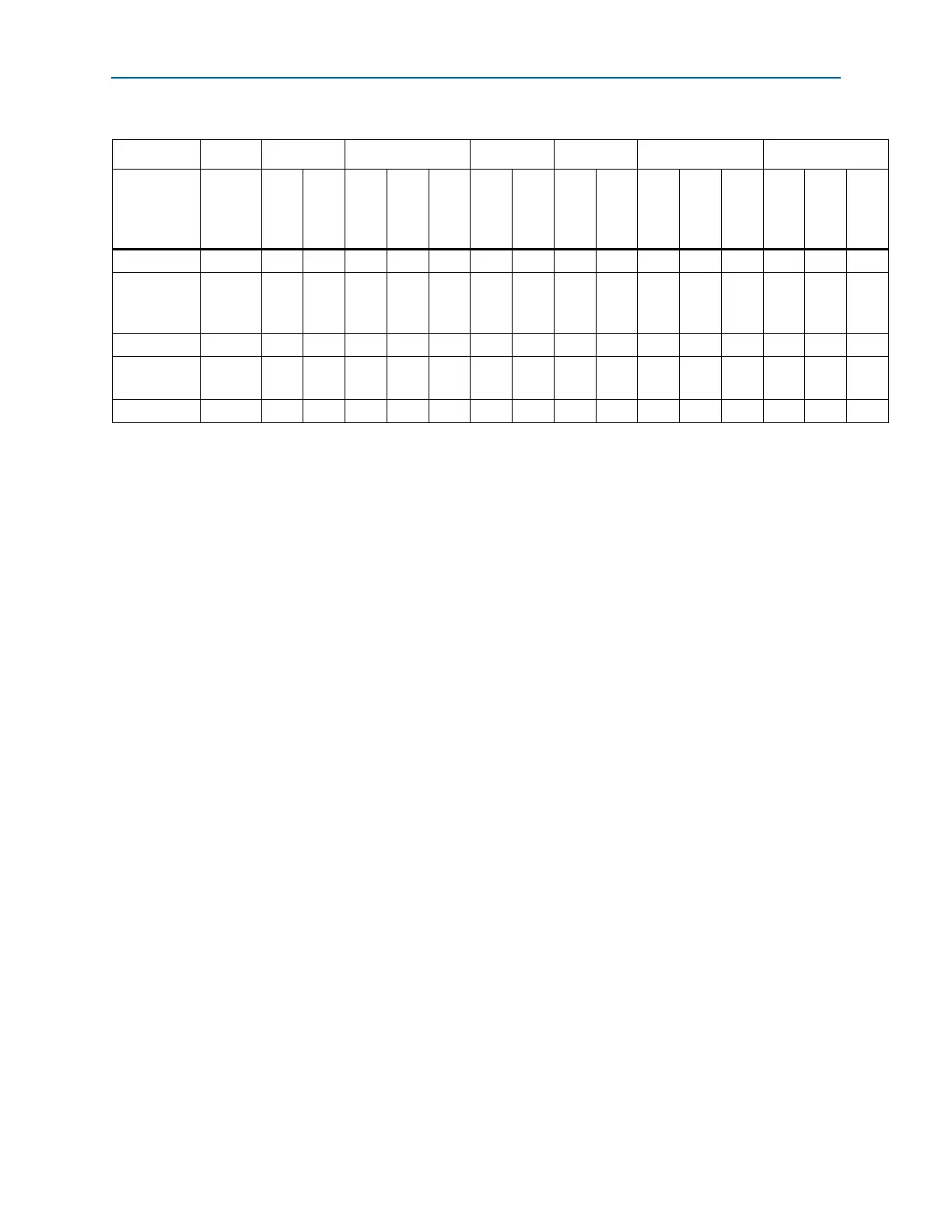
Table 6–9. Cyclone IV GX I/O, Differential, and XCVRs Channel Count
Device 4CGX15 4CGX22 4CGX30 4CGX50 4CGX75 4CGX110 4CGX150
Numbers of
Differential
Channels
(1),
(2)
169-FBGA
169-FBGA
324-FBGA
169-FBGA
324-FBGA
484-FBGA
484-FBGA
672-FBGA
484-FBGA
672-FBGA
484-FBGA
672-FBGA
896-FBGA
484-FBGA
672-FBGA
896-FBGA
User I/O
(3)
72 72 150 72 150 290 290 310 290 310 270 393 475 270 393 475
User I/O
banks
9
(4)
9
(4)
9
(4)
9
(4)
9
(4)
11
(5)
11
(5)
,
(6)
11
(5),
(6)
11
(5),
(6)
11
(5),
(6)
11
(5),
(6)
11
(5),
(6)
11
(5),
(6)
11
(5),
(6)
11
(5),
(6)
11
(5),
(6)
LVDS
(7), (9)
9 9 16 9 164545514551385263385263
Emulated
LVDS
(8), (9)
16 16 48 16 48 85 85 89 85 89 82 129 157 82 129 157
XCVRs 2 242444848488488
Notes to Table 6–9:
(1) User I/O pins are used as inputs or outputs; clock input pins are used as inputs only; clock output pins are used as outputs only.
(2) For differential pad placement guidelines, refer to “Pad Placement” on page 6–23.
(3) The I/O pin count includes all GPIOs, dedicated clock pins, and dual-purpose configuration pins. Transceivers pins and dedicated configuration pins are
not included in the pin count.
(4) Includes one configuration I/O bank and two dedicated clock input I/O banks for HSSI input reference clock.
(5) Includes one configuration I/O bank and four dedicated clock input I/O banks for HSSI input reference clock.
(6) Single-ended clock input support is available for dedicated clock input I/O banks 3B (pins
CLKIO20
and
CLKIO22
) and 8B (pins
CLKIO17
and
CLKIO19
).
(7) The true LVDS count includes all LVDS I/O pairs, differential clock input and clock output pins in right I/O banks 5 and 6.
(8) The emulated LVDS count includes all LVDS I/O pairs, differential clock input and clock output pins in column I/O banks 3, 4, 7, and 8.
(9) LVDS input and output buffers are sharing the same p and n pins. One LVDS I/O channel can only be either transmitter or receiver at a time.