Chapter 1: Cyclone IV Transceivers Architecture 1–11
Receiver Channel Datapath
February 2015 Altera Corporation Cyclone IV Device Handbook,
Volume 2
Receiver Channel Datapath
The following sections describe the Cyclone IV GX receiver channel datapath
architecture as shown in Figure 1–3 on page 1–4:
■ “Receiver Input Buffer” on page 1–11
■ “Clock Data Recovery” on page 1–15
■ “Deserializer” on page 1–16
■ “Word Aligner” on page 1–17
■ “Deskew FIFO” on page 1–22
■ “Rate Match FIFO” on page 1–23
■ “8B/10B Decoder” on page 1–23
■ “Byte Deserializer” on page 1–24
■ “Byte Ordering” on page 1–24
■ “RX Phase Compensation FIFO” on page 1–25
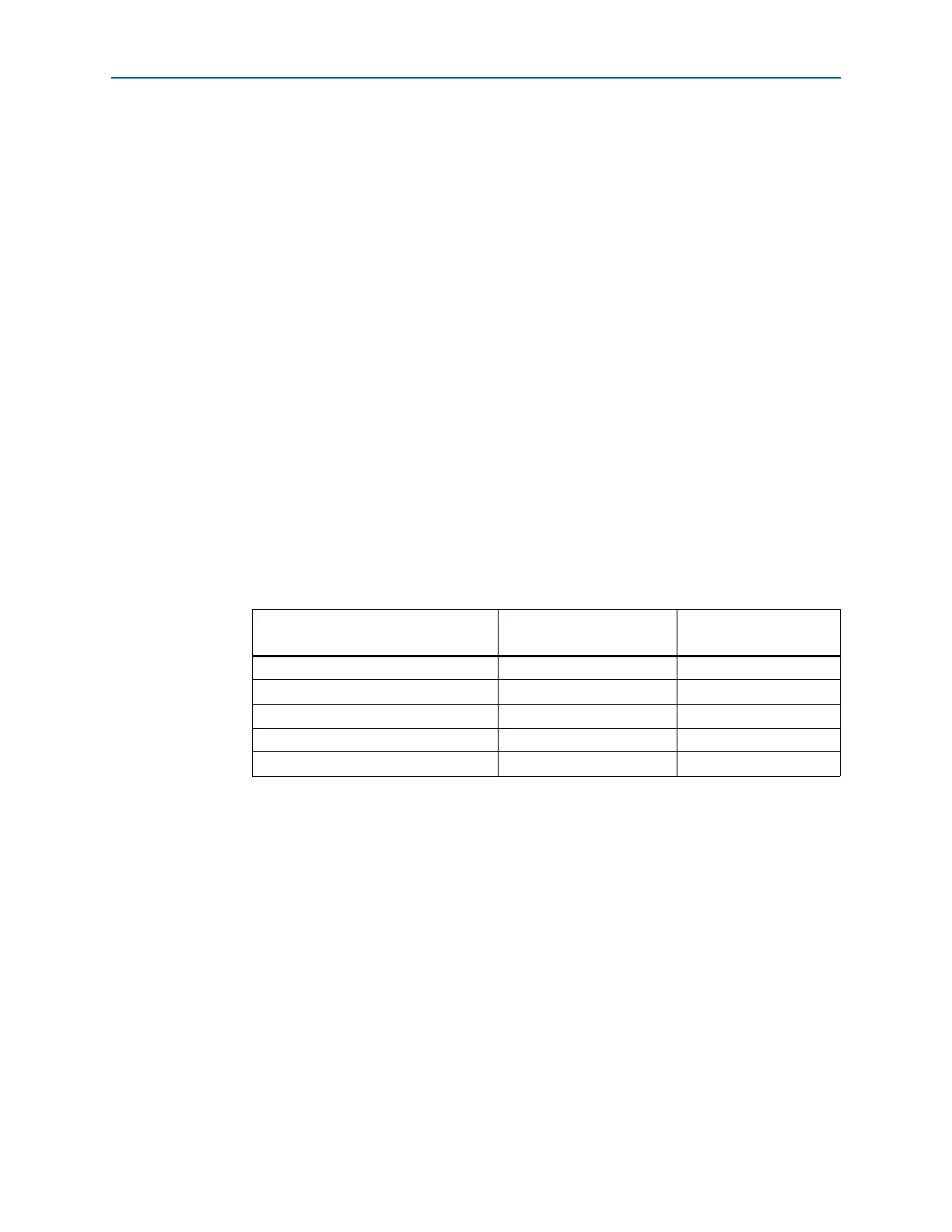
Receiver Input Buffer
Table 1–2 lists the electrical features supported by the Cyclone IV GX receiver input
buffer.
Table 1–2. Electrical Features Supported by the Receiver Input Buffer
I/O Standard
Programmable Common
Mode Voltage (V)
Coupling
1.4-V PCML 0.82 AC, DC
1.5-V PCML 0.82 AC, DC
2.5-V PCML 0.82 AC
LVPECL 0.82 AC
LVDS 0.82 AC, DC
(1)
Note to Table 1–2:
(1) DC coupling is supported for LVDS with lower on-chip common mode voltage of 0.82 V.