Chapter 6: I/O Features in Cyclone IV Devices 6–29
High-Speed I/O Standards Support
March 2016 Altera Corporation Cyclone IV Device Handbook,
Volume 1
The
CLKIN/REFCLK
pins are powered by dedicated V
CC_CLKIN3A
, V
CC_CLKIN3B
,
V
CC_CLKIN8A
, and V
CC_CLKIN8B
power supplies separately in their respective I/O banks
to avoid the different power level requirements in the same bank for GPIO.
f For more information about the AC-coupled termination scheme for the HSSI
reference clock, refer to the Cyclone IV Transceivers Architecture chapter.
LVDS I/O Standard Support in Cyclone IV Devices
The LVDS I/O standard is a high-speed, low-voltage swing, low power, and GPIO
interface standard. Cyclone IV devices meet the ANSI/TIA/EIA-644 standard with
the following exceptions:
■ The maximum differential output voltage (V
OD
) is increased to 600 mV. The
maximum V
OD
for ANSI specification is 450 mV.
■ The input voltage range is reduced to the range of 1.0 V to 1.6 V, 0.5 V to 1.85 V, or
0 V to 1.8 V based on different frequency ranges. The ANSI/TIA/EIA-644
specification supports an input voltage range of 0 V to 2.4 V.
f For LVDS I/O standard electrical specifications in Cyclone IV devices, refer to the
Cyclone IV Device Datasheet chapter.
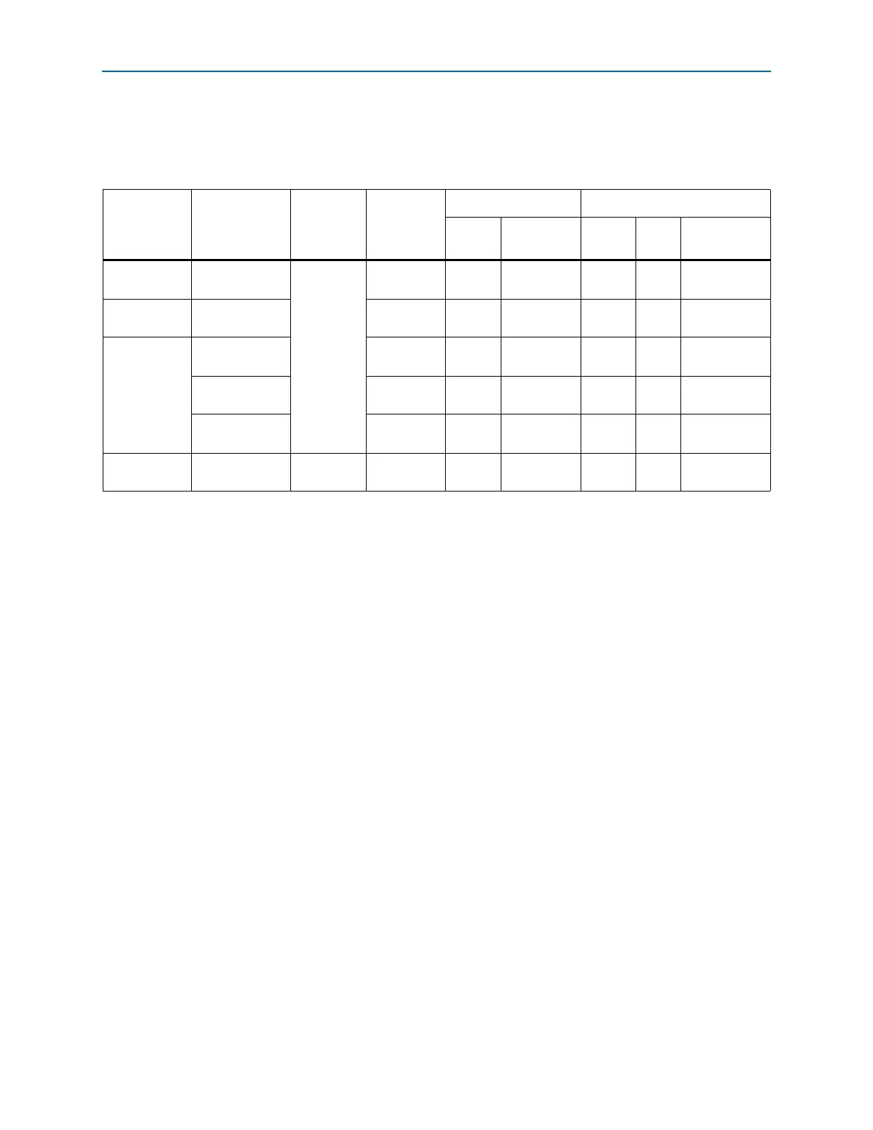
Table 6–10. Cyclone IV GX HSSI REFCLK I/O Standard Support Using GPIO CLKIN Pins
(1),
(2)
I/O Standard HSSI Protocol Coupling Termination
VCC_CLKIN Level I/O Pin Type
Input Output
Column
I/O
Row
I/O
Supported I/O
Banks
LVDS All
Differential
AC (Need
off chip
resistor to
restore
V
CM
)
Off chip 2.5V
Not
supported
Yes No 3A, 3B, 8A, 8B
LVPECL All Off chip 2.5V
Not
supported
Yes No 3A, 3B, 8A, 8B
1.2V, 1.5V,
3.3V PCML
All Off chip 2.5V
Not
supported
Yes No 3A, 3B, 8A, 8B
All Off chip 2.5V
Not
supported
Yes No 3A, 3B, 8A, 8B
All Off chip 2.5V
Not
supported
Yes No 3A, 3B, 8A, 8B
HCSL PCIe
Differential
DC
Off chip 2.5V
Not
supported
Yes No 3A, 3B, 8A, 8B
Notes to Table 6–10:
(1) The EP4CGX15, EP4CGX22, and EP4CGX30 devices have two pairs of dedicated clock input pins in banks 3A and 8A for HSSI input reference
clock. I/O banks 3B and 8B are not available in EP4CGX15, EP4CGX22, and EP4CGX30 devices.
(2) The EP4CGX50, EP4CGX75, EP4CGX110, and EP4CGX150 devices have four pairs of dedicated clock input pins in banks 3A, 3B, 8A, and 8B
for HSSI input or single-ended clock input.