Chapter 8: Configuration and Remote System Upgrades in Cyclone IV Devices 8–5
Configuration
May 2013 Altera Corporation Cyclone IV Device Handbook,
Volume 1
Use the data in Table 8–2 to estimate the file size before design compilation. Different
configuration file formats, such as Hexadecimal (.hex) or Tabular Text File (.ttf)
formats, have different file sizes. However, for any specific version of the Quartus II
software, any design targeted for the same device has the same uncompressed
configuration file size. If you use compression, the file size varies after each
compilation, because the compression ratio depends on the design.
f For more information about setting device configuration options or creating
configuration files, refer to the Software Settings section in volume 2 of the
Configuration Handbook.
Configuration and JTAG Pin I/O Requirements
Cyclone IV devices are manufactured using the TSMC 60-nm low-k dielectric process.
Although Cyclone IV devices use TSMC 2.5-V transistor technology in the I/O
buffers, the devices are compatible and able to interface with 2.5, 3.0, and 3.3-V
configuration voltage standards by following specific requirements.
All I/O inputs must maintain a maximum AC voltage of 4.1 V. When using a serial
configuration device in an AS configuration scheme, you must connect a 25- series
resistor for the
DATA[0]
pin. When cascading the Cyclone IV device family in a
multi-device configuration for AS, AP, FPP, and PS configuration schemes, you must
connect the repeater buffers between the master and slave devices for the
DATA
and
DCLK
pins. When using the JTAG configuration scheme in a multi-device
configuration, connect 25- resistors on both ends of the
TDO-TDI
path if the
TDO
output driver is a non-Cyclone IV device.
The output resistance of the repeater buffers and the
TDO
path for all cases must fit the
maximum overshoot equation shown in Equation 8–1.
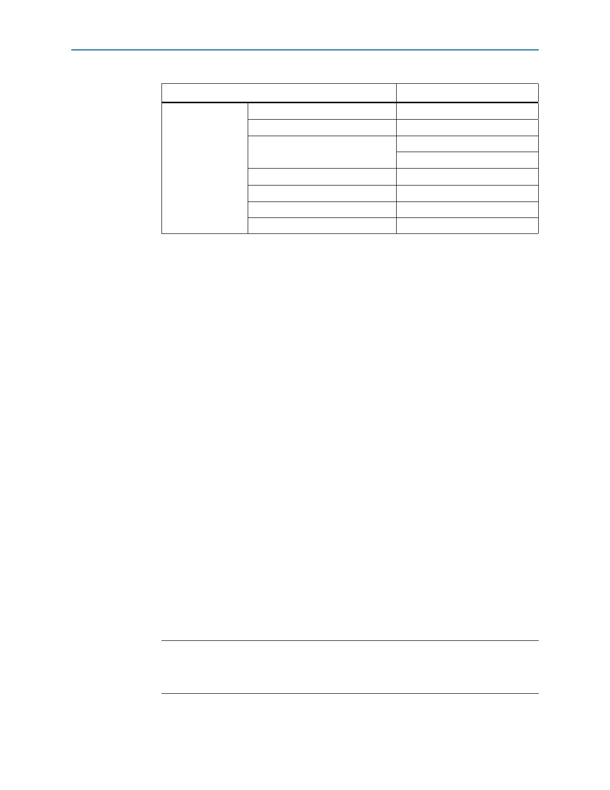
Cyclone IV GX
EP4CGX15 3,805,568
EP4CGX22 7,600,040
EP4CGX30
7,600,040
22,010,888
(1)
EP4CGX50 22,010,888
EP4CGX75 22,010,888
EP4CGX110 39,425,016
EP4CGX150 39,425,016
Note to Table 8–2:
(1) Only for the F484 package.
Table 8–2. Uncompressed Raw Binary File (.rbf) Sizes for Cyclone IV Devices (Part 2 of 2)
Device Data Size (bits)
Equation 8–1.
(1)
Note to Equation 8–1:
(1) Z
O
is the transmission line impedance and R
E
is the equivalent resistance of the output buffer.