Chapter 1: Cyclone IV Transceivers Architecture 1–29
Transceiver Clocking Architecture
February 2015 Altera Corporation Cyclone IV Device Handbook,
Volume 2
Figure 1–27 shows an example of the termination scheme for AC-coupled connections
for
REFCLK
pins.
Figure 1–28 shows an example termination scheme for the
REFCLK
pin when
configured as a HCSL input.
Transceiver Channel Datapath Clocking
Channel datapath clocking varies with channel configuration options and PCS
configurations. This section describes the clock distribution from the left PLLs for
transceiver channels and the datapath clocking in various supported configurations.
Table 1–7 lists the clocks generated by the PLLs for transceiver datapath.
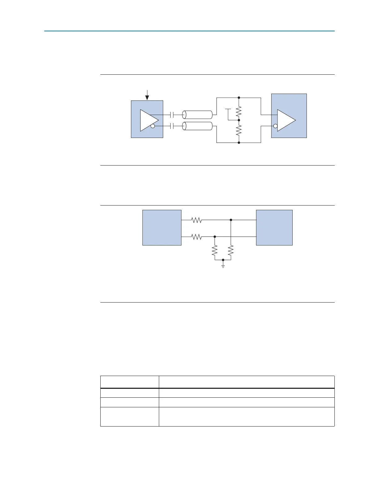
Figure 1–27. AC-Coupled Termination Scheme for a Reference Clock
Note to Figure 1–27:
(1) For more information about the V
ICM
value, refer to the Cyclone IV Device Datasheet chapter.
Figure 1–28. Termination Scheme for a Reference Clock When Configured as HCSL
(1)
Notes to Figure 1–28:
(1) No biasing is required if the reference clock signals are generated from a clock source that conforms to the PCIe
specification.
(2) Select values as recommended by the PCIe clock source vendor.
Z
0
= 50 Ω
Z
0
= 50 Ω
50 Ω
LVDS, LVPECL, PCML
(1.2 V, 1.5 V, 3.3 V)
50 Ω
Cyclone IV GX
REFCLK
0.1 μF
0.1 μF
V
ICM
PCI Express
(HCSL)
REFCLK
Source
REFCLK +
REFCLK -
Cyclone IV GX
Rs
Rs
50 Ω 50 Ω
(2)
(2)
Table 1–7. PLL Clocks for Transceiver Datapath
Clock Usage
CDR clocks Receiver CDR unit
High-speed clock Transmitter serializer block in PMA
Low-speed clock
Transmitter PCS blocks
Receiver PCS blocks when rate match FIFO enabled