Chapter 1: Cyclone IV Transceivers Architecture 1–83
Self Test Modes
February 2015 Altera Corporation Cyclone IV Device Handbook,
Volume 2
PRBS
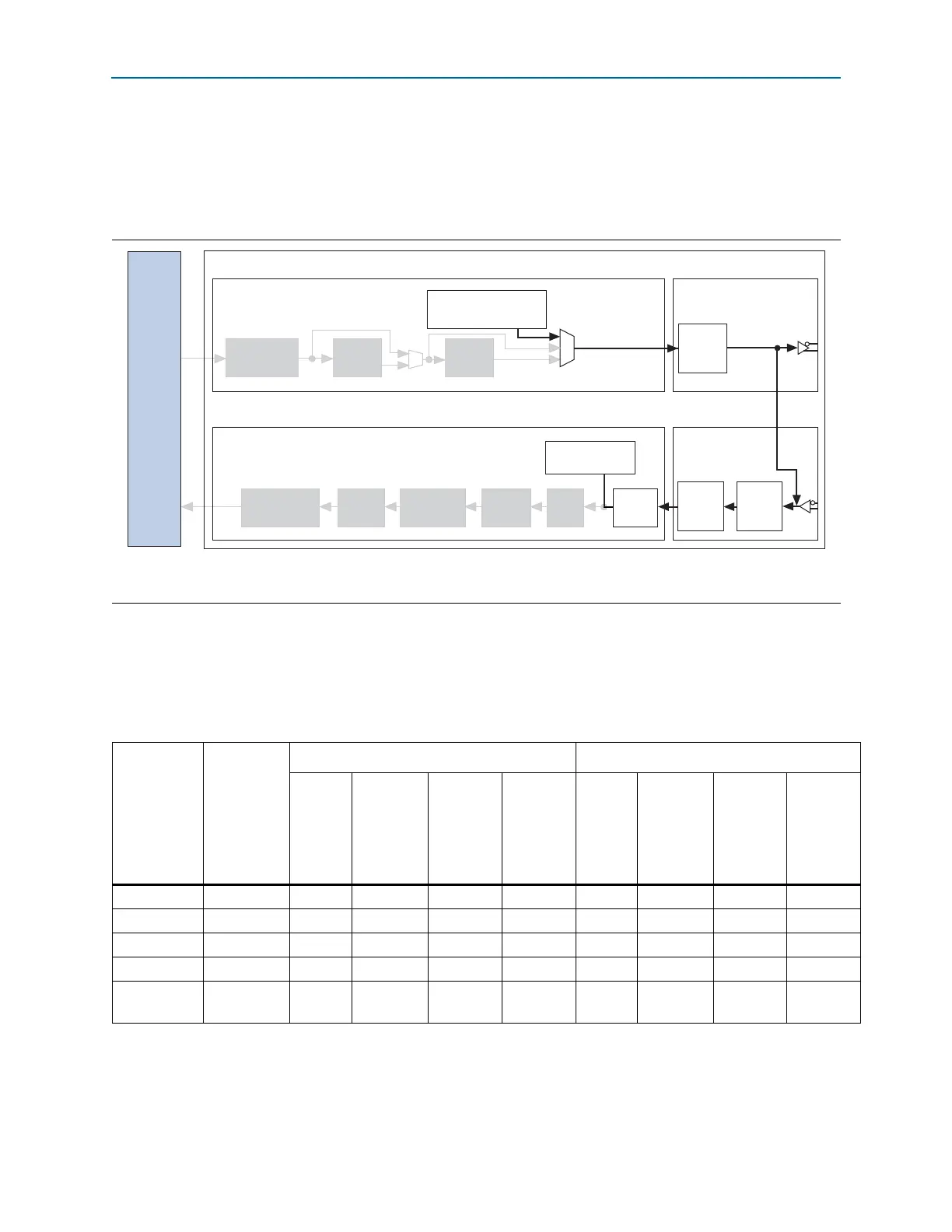
Figure 1–74 shows the datapath for the PRBS, high and low frequency pattern test
modes. The pattern generator is located in TX PCS before the serializer, and PRBS
pattern verifier located in RX PCS after the word aligner.
Table 1–25 lists the supported PRBS, high and low frequency patterns, and
corresponding channel settings. The PRBS pattern repeats after completing an
iteration. The number of bits a PRBS X pattern sends before repeating the pattern is
2
(X-1)
bits.
Figure 1–74. PRBS Pattern Test Mode Datapath
Note to Figure 1–74:
(1) Serial loopback path is optional and can be enabled for the PRBS verifier to check the PRBS pattern
Transceiver
Receiver Channel
PMA
Transmitter Channel PMA
Receiver Channel PCS
Transmitter Channel PCS
Tx Phase
Compensation
FIFO
PRBS, High Freq,
Low Freq Pattern
Generator
8B/10B
Encoder
Byte
Serializer
Rx
Compensation
FIFO
PRBS
Verifier
8B/10B
Decoder
Rate
Match
FIFO
Word
Aligner
Byte
Deserializer
Byte
Ordering
(1)
De-
serializer
Serializer
Receiver
CDR
FPGA
Fabric
Table 1–25. PRBS, High and Low Frequency Patterns, and Channel Settings (Part 1 of 2)
Patterns Polynomial
8-bit Channel Width 10-bit Channel Width
Channel
Width
of
8bits
(1)
Word
Alignment
Pattern
Maximum
Data Rate
(Gbps) for
F324 and
Smaller
Packages
Maximum
Data Rate
(Gbps) for
F484 and
Larger
Packages
Channel
Width
of
10-bits
(1)
Word
Alignment
Pattern
Maximum
Data Rate
(Gbps) for
F324 and
Smaller
Packages
Maximum
Data Rate
(Gbps) for
F484 and
Larger
Packages
PRBS 7 X
7
+ X
6
+ 1 Y 16’h3040 2.0 2.5 N — — —
PRBS 8 X
8
+ X
7
+ 1 Y 16’hFF5A 2.0 2.5 N — — —
PRBS 10 X
10
+ X
7
+ 1 N — — — Y 10’h3FF 2.5 3.125
PRBS 23 X
23
+ X
18
+ 1 Y 16’hFFFF 2.0 2.5 N — — —
High
frequency
(2)
1010101010 Y — 2.0 2.5 Y — 2.5 3.125