Chapter 6: I/O Features in Cyclone IV Devices 6–37
Design Guidelines
March 2016 Altera Corporation Cyclone IV Device Handbook,
Volume 1
Figure 6–22 shows the Cyclone IV devices high-speed I/O timing budget.
f For more information, refer to the Cyclone IV Device Datasheet chapter.
Design Guidelines
This section provides guidelines for designing with Cyclone IV devices.
Differential Pad Placement Guidelines
To maintain an acceptable noise level on the V
CCIO
supply, you must observe some
restrictions on the placement of single-ended I/O pins in relation to differential pads.
1 For guidelines on placing single-ended pads with respect to differential pads in
Cyclone IV devices, refer to “Pad Placement and DC Guidelines” on page 6–23.
Input jitter tolerance (peak-to-peak) —
Allowed input jitter on the input clock to the PLL that is tolerable
while maintaining PLL lock.
Output jitter (peak-to-peak) — Peak-to-peak output jitter from the PLL.
Note to Table 6–11:
(1) The TCCS specification applies to the entire bank of differential I/O as long as the SERDES logic is placed in the logic array block (LAB) adjacent
to the output pins.
Table 6–11. High-Speed I/O Timing Definitions (Part 2 of 2)
Parameter Symbol Description
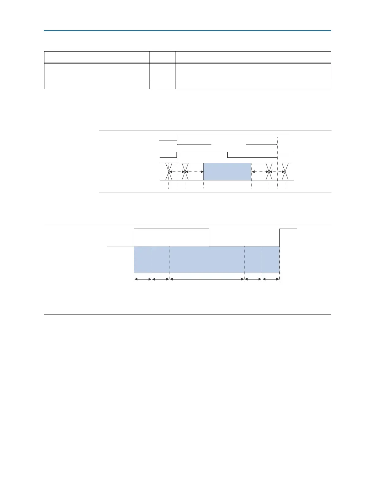
Figure 6–21. High-Speed I/O Timing Diagram
Sampling Window (SW)
Time Unit Interval (TUI)
RSKM TCCSRSKMTCCS
Internal Clock
External
Input Clock
Receiver
Input Data
Figure 6–22. Cyclone IV Devices High-Speed I/O Timing Budget
(1)
Note to Figure 6–22:
(1) The equation for the high-speed I/O timing budget is:
Internal Clock Period
RSKM
0.5 × TCCS
RSKM
0.5 × TCCS
SW
eriod 0.5 TCCS RSKM SW RSKM 0.5 TCCS++++=