5–12 Chapter 5: Clock Networks and PLLs in Cyclone IV Devices
Clock Networks
Cyclone IV Device Handbook, October 2012 Altera Corporation
Volume 1
GCLK Network Clock Source Generation
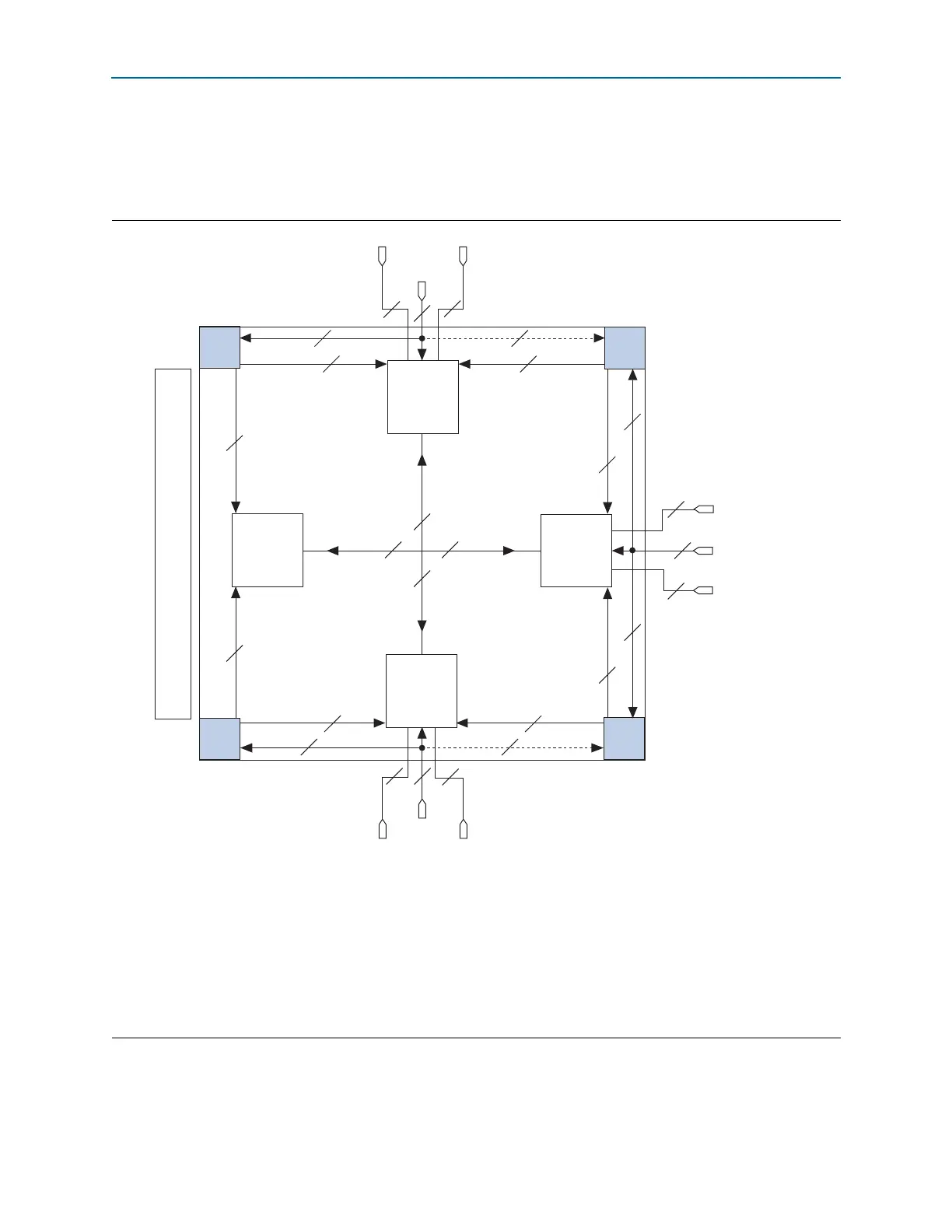
Figure 5–2, Figure 5–3, and Figure 5–4 on page 5–14 show the Cyclone IV PLLs, clock
inputs, and clock control block location for different Cyclone IV device densities.
Figure 5–2. Clock Networks and Clock Control Block Locations in EP4CGX15, EP4CGX22, and EP4CGX30 Devices
(1),
(2)
Notes to Figure 5–2:
(1) The clock networks and clock control block locations apply to all EP4CGX15, EP4CGX22, and EP4CGX30 devices except EP4CGX30 device in F484
package.
(2)
PLL_1
and
PLL_2
are multipurpose PLLs while
PLL_3
and
PLL_4
are general purpose PLLs.
(3) There are five clock control blocks on each side.
(4)
PLL_4
is only available in EP4CGX22 and EP4CGX30 devices in F324 package.
(5) The EP4CGX15 device has two
DPCLK
pins on three sides of the device:
DPCLK2
and
DPCLK5
on bottom side,
DPCLK7
and
DPCLK8
on the right
side,
DPCLK10
and
DPCLK13
on the top side of device.
(6) Dedicated clock pins can feed into this PLL. However, these paths are not fully compensated.
PLL_
1
PLL_3
PLL_4
PLL_
2
20
20
20
20
4
4
4
22
22
2
2
5
5
DPCLK[13..12]
(5)
DPCLK[11..10]
(5)
CLK[11..8]
GCLK[19..0]
GCLK[19..0]
DPCLK[9..8]
(5)
CLK[7..4]
DPCLK[7..6]
(5)
DPCLK[3..2]
(5)
CLK[15..12]
DPCLK[5..4]
(5)
(4)
(6)
HSSI
4
5
4
5
4
5
4
5
4
5
4
5
Clock
Control
Block (3)
Clock
Control
Block (3)
Clock
Control
Block (3)
Clock
Control
Block (3)
(6)