5–14 Chapter 5: Clock Networks and PLLs in Cyclone IV Devices
Clock Networks
Cyclone IV Device Handbook, October 2012 Altera Corporation
Volume 1
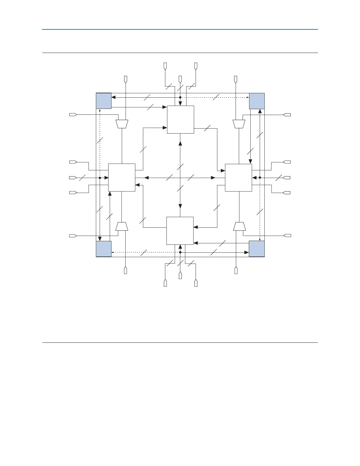
The inputs to the clock control blocks on each side of the Cyclone IV GX device must
be chosen from among the following clock sources:
■ Four clock input pins
■ Ten PLL counter outputs (five from each adjacent PLLs)
■ Two, four, or six
DPCLK
pins from the top, bottom, and right sides of the device
■ Five signals from internal logic
Figure 5–4. Clock Networks and Clock Control Block Locations in Cyclone IV E Devices
Notes to Figure 5–4:
(1) There are five clock control blocks on each side.
(2) Only one of the corner
CDPCLK
pins in each corner can feed the clock control block at a time. You can use the other
CDPCLK
pins as
general-purpose I/O (GPIO) pins.
(3) Dedicated clock pins can feed into this PLL. However, these paths are not fully compensated.
(4)
PLL_3
and
PLL_4
are not available in EP4CE6 and EP4CE10 devices.
PLL_1
PLL_4
PLL_2
PLL_3
20
20
20
20
4
4
4
4
3
4
4
4
2
2
2
2
22
22
5
5
5
5
(2)(2)
(2) (2)
CDPCLK7
CDPCLK0
CDPCLK1
DPCLK1
DPCLK[11.10]
DPCLK[9..8]
CLK[11..8]
CDPCLK6
DPCLK0
CLK[3..1]
GCLK[19..0]
GCLK[19..0]
CDPCLK5
DPCLK7
CLK[7..4]
DPCLK6
CDPCLK4
CDPCLK2
DPCLK[3..2]
CLK[15..12]
DPCLK[5..4]
CDPCLK3
4
4
4
4
(3)
(3)
(3)
(4)
(4)
(3)
Clock
Control
Block (1)
Clock
Control
Block (1)
Clock
Control
Block (1)
Clock
Control
Block (1)