Chapter 5: Clock Networks and PLLs in Cyclone IV Devices 5–13
Clock Networks
October 2012 Altera Corporation Cyclone IV Device Handbook,
Volume 1
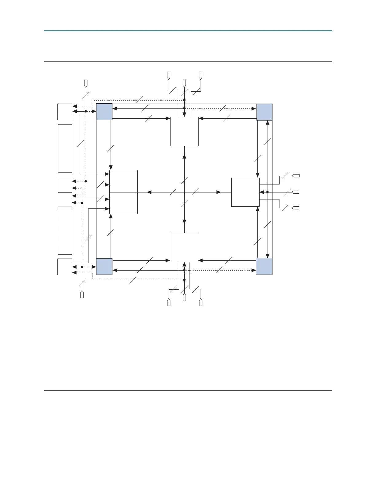
Figure 5–3. Clock Networks and Clock Control Block Locations in EP4CGX30, EP4CGX50, EP4CGX75, EP4CGX110, and
EP4CGX150 Devices
(1),
(2)
Notes to Figure 5–3:
(1) The clock networks and clock control block locations in this figure apply to only the EP4CGX30 device in F484 package and all EP4CGX50,
EP4CGX75, EP4CGX110, and EP4CGX150 devices.
(2)
PLL_1
,
PLL_2
,
PLL_3
, and
PLL_4
are general purpose PLLs while
PLL_5
,
PLL_6
,
PLL_7
, and
PLL_8
are multipurpose PLLs.
(3) There are 6 clock control blocks on the top, right and bottom sides of the device and 12 clock control blocks on the left side of the device.
(4)
REFCLK[0,1]p/n
and
REFCLK[4,5]p/n
can only drive the general purpose PLLs and multipurpose PLLs on the left side of the device. These
clock pins do not have access to the clock control blocks and GCLK networks. The
REFCLK[4,5]p/n
pins are not available in devices in F484
package.
(5) Not available for EP4CGX30, EP4CGX50, EP4CGX75, EP4CGX110, and EP4CGX150 devices in F484 package.
(6) Dedicated clock pins can feed into this PLL. However, these paths are not fully compensated.
PLL_
1
PLL_3
PLL_4PLL_
2
30
30
30
30
4
4
4
4
4
4
33
33
3
3
4
5
4
4
5
5
4
5
5
5
DPCLK[17..15]
DPCLK[14..12]
CLKIO[11..8]
GCLK[29..0]
GCLK[29..0]
DPCLK[11..9]
CLKIO[7..4]
DPCLK[8..6]
DPCLK[2..0]
CLKIO[15..12]
REFCLK[0,1]p/n (4)
REFCLK[4,5]p/n (4)
DPCLK[5..3]
Clock
Control
Block (3)
Clock
Control
Block (3)
Clock
Control
Block (3)
Clock
Control
Block (3)
Clock
Control
Block (3)
3
3
2
2
4
4
5
4
5
HSSI
HSSI
PLL_
8
(5)
PLL_
5
PLL_
7
(5)
PLL_
6
(6)
(6)
(6)
(6)
(6)
(6)
(6)
(6)