7–2 Chapter 7: External Memory Interfaces in Cyclone IV Devices
Cyclone IV Devices Memory Interfaces Pin Support
Cyclone IV Device Handbook, March 2016 Altera Corporation
Volume 1
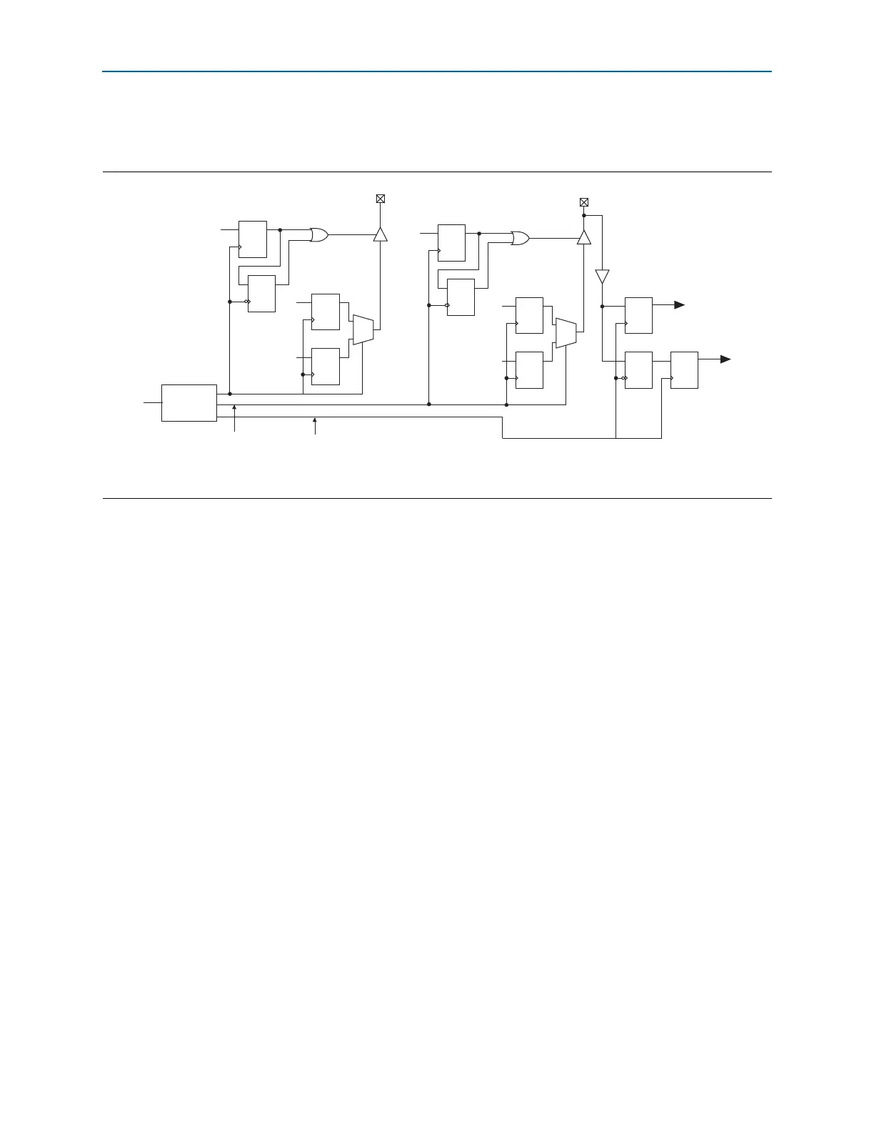
Figure 7–1 shows the block diagram of a typical external memory interface data path
in Cyclone IV devices.
f For more information about implementing complete external memory interfaces, refer
to the External Memory Interface Handbook.
Cyclone IV Devices Memory Interfaces Pin Support
Cyclone IV devices use data (DQ), data strobe (DQS), clock, command, and address
pins to interface with external memory. Some memory interfaces use the data mask
(DM) or byte write select (BWS#) pins to enable data masking. This section describes
how Cyclone IV devices support all these different pins.
f For more information about pin utilization, refer to Volume 2: Device, Pin, and Board
Layout Guidelines of the External Memory Interface Handbook.
Data and Data Clock/Strobe Pins
Cyclone IV data pins for external memory interfaces are called D for write data, Q for
read data, or
DQ
for shared read and write data pins. The read-data strobes or read
clocks are called
DQS
pins. Cyclone IV devices support both bidirectional data strobes
and unidirectional read clocks. Depending on the external memory standard, the
DQ
and
DQS
are bidirectional signals (in DDR2 and DDR SDRAM) or unidirectional
signals (in QDR II SRAM). Connect the bidirectional
DQ
data signals to the same
Cyclone IV devices
DQ
pins. For unidirectional
D
or
Q
signals, connect the read-data
signals to a group of
DQ
pins and the write-data signals to a different group of
DQ
pins.
1 In QDR II SRAM, the Q read-data group must be placed at a different V
REF
bank
location from the D write-data group, command, or address pins.
Figure 7–1. Cyclone IV Devices External Memory Data Path
(1)
Note to Figure 7–1:
(1) All clocks shown here are global clocks.
DQS/CQ/CQn
OE
V
CC
PLL
GND
System Clock
DQ
OE
DataA
DataB
-90° Shifted Clock
IOE
Register
IOE
Register
IOE
Register
IOE
Register
IOE
Register
IOE
Register
IOE
Register
LE
Register
LE
Register
LE
Register
IOE
Register
Capture Clock