Chapter 5: Clock Networks and PLLs in Cyclone IV Devices 5–21
Cyclone IV PLL Hardware Overview
October 2012 Altera Corporation Cyclone IV Device Handbook,
Volume 1
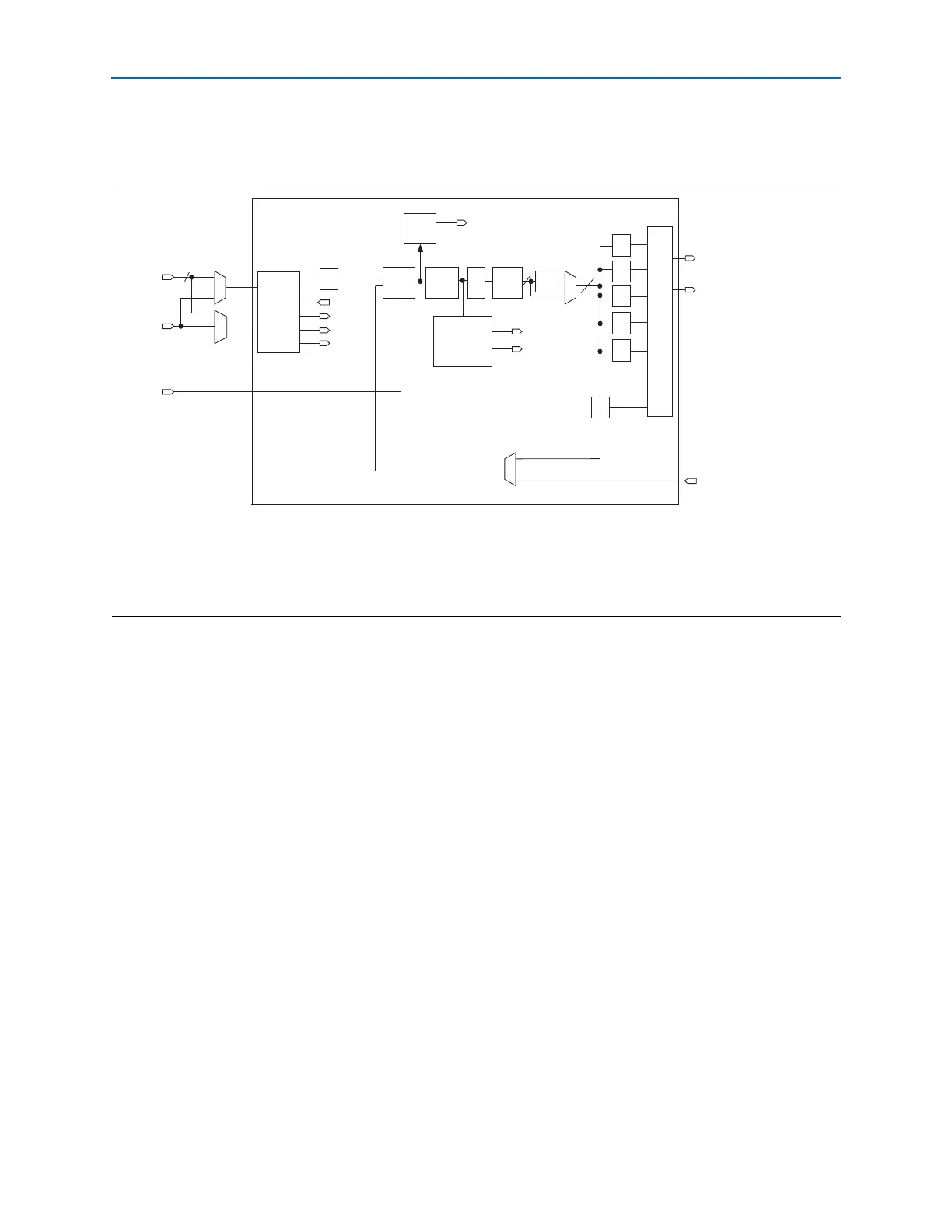
Figure 5–10 shows a simplified block diagram of the major components of the PLL of
Cyclone IV E devices.
1 The VCO post-scale counter K is used to divide the supported VCO range by two. The
VCO frequency reported by the Quartus II software in the PLL summary section of
the compilation report takes into consideration the VCO post-scale counter value.
Therefore, if the VCO post-scale counter has a value of 2, the frequency reported is
lower than the f
VCO
specification specified in the Cyclone IV Device Datasheet chapter.
External Clock Outputs
Each PLL of Cyclone IV devices supports one single-ended clock output or one
differential clock output. Only the C0 output counter can feed the dedicated external
clock outputs, as shown in Figure 5–11, without going through the GCLK. Other
output counters can feed other I/O pins through the GCLK.
Figure 5–10. Cyclone IV E PLL Block Diagram
(1)
Notes to Figure 5–10:
(1) Each clock source can come from any of the four clock pins located on the same side of the device as the PLL.
(2) This is the VCO post-scale counter K.
(3) This input port is fed by a pin-driven dedicated GCLK, or through a clock control block if the clock control block is fed by an output from another
PLL or a pin-driven dedicated GCLK. An internally generated global signal cannot drive the PLL.
Clock
Switchover
Block
inclk0
inclk1
Clock inputs
from pins
GCLK
pfdena
clkswitch
clkbad0
clkbad1
activeclock
PFD
LOCK
circuit
lock
÷n
CP LF VCO
÷2
(2)
÷C0
÷C1
÷C2
÷C3
÷C4
÷M
PLL
output
mux
GCLKs
External clock output
8
8
4
GCLK networks
no compensation;
ZDB mode
source-synchronous;
normal mode
VCO
Range
Detector
VCOOVRR
VCOUNDR
(3)