5–22 Chapter 5: Clock Networks and PLLs in Cyclone IV Devices
Cyclone IV PLL Hardware Overview
Cyclone IV Device Handbook, October 2012 Altera Corporation
Volume 1
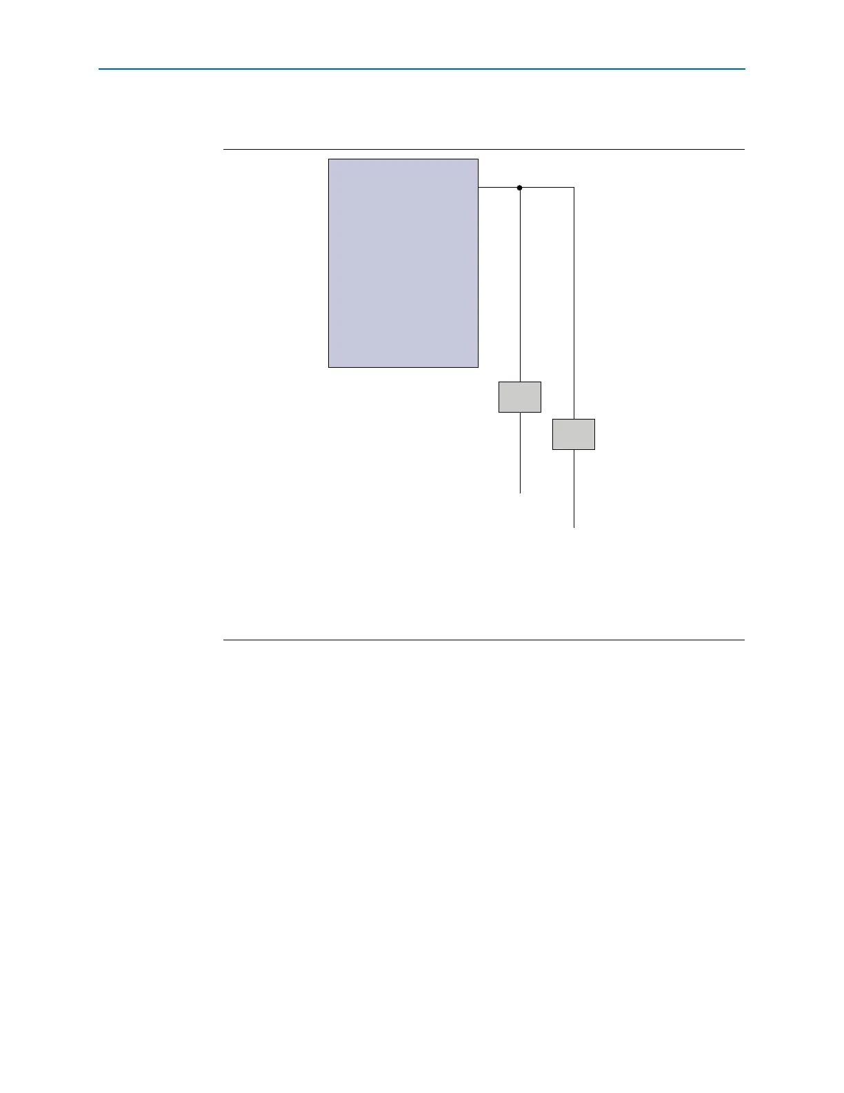
Figure 5–11 shows the external clock outputs for PLLs.
Each pin of a differential output pair is 180° out of phase. The Quartus II software
places the NOT gate in your design into the I/O element to implement 180° phase
with respect to the other pin in the pair. The clock output pin pairs support the same
I/O standards as standard output pins.
f To determine which I/O standards are supported by the PLL clock input and output
pins, refer to the Cyclone IV Device I/O Features chapter.
Cyclone IV PLLs can drive out to any regular I/O pin through the GCLK. You can also
use the external clock output pins as GPIO pins if external PLL clocking is not
required.
Figure 5–11. External Clock Outputs for PLLs
Notes to Figure 5–11:
(1) These external clock enable signals are available only when using the ALTCLKCTRL megafunction.
(2)
PLL#_CLKOUTp
and
PLL#_CLKOUTn
pins are dual-purpose I/O pins that you can use as one single-ended clock
output or one differential clock output. When using both pins as single
-ended I/Os, one of them can be the clock
output while the other pin is configured as a regular user I/O.
C0
C1
C2
C4
C3
PLL#
clkena 1
(1
clkena 0
(1)
PLL#_CLKOUTp
(2)
PLL#_CLKOUTn
(2)