1–10 Chapter 1: Cyclone IV Transceivers Architecture
Transmitter Channel Datapath
Cyclone IV Device Handbook, February 2015 Altera Corporation
Volume 2
Transmitter Output Buffer
Figure 1–11 shows the transmitter output buffer block diagram.
The Cyclone IV GX transmitter output buffers support the 1.5-V PCML I/O standard
and are powered by
VCCH_GXB
power pins with 2.5-V supply. The 2.5-V supply on
VCCH_GXB
pins are regulated internally to 1.5-V for the transmitter output buffers. The
transmitter output buffers support the following additional features:
■ Programmable differential output voltage (V
OD
)—customizes the V
OD
up to
1200 mV to handle different trace lengths, various backplanes, and various
receiver requirements.
■ Programmable pre-emphasis—boosts high-frequency components in the
transmitted signal to maximize the data eye opening at the far-end. The
high-frequency components might be attenuated in the transmission media due to
data-dependent jitter and intersymbol interference (ISI) effects. The requirement
for pre-emphasis increases as the data rates through legacy backplanes increase.
■ Programmable differential on-chip termination (OCT)—provides calibrated OCT
at differential 100 or 150 with on-chip transmitter common mode voltage
(V
CM
) at 0.65 V. V
CM
is tri-stated when you disable the OCT to use external
termination.
1 Disable OCT to use external termination if the link requires a 85 termination, such
as when you are interfacing with certain PCIe Gen1 or Gen2 capable devices.
f The Cyclone IV GX transmitter output buffers are current-mode drivers. The resulting
V
OD
voltage is therefore a function of the transmitter termination value. For lists of
supported V
OD
settings, refer to the Cyclone IV Device Data Sheet.
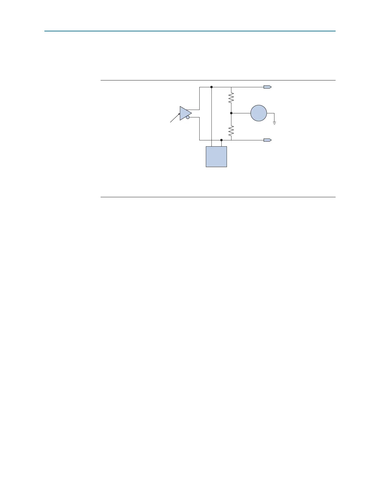
Figure 1–11. Transmitter Output Buffer Block Diagram
Note to Figure 1–11:
(1) Receiver detect function is specific for PCIe protocol implementation only. For more information, refer to “PCI
Express (PIPE) Mode” on page 1–52.
GXB_TXp
GXB_TXn
Programmable
Pre-emphasis
and V
OD
Receiver
Detect
(1)
50 or 75
50 or 75
+ V
CM
-