3–6 Chapter 3: Memory Blocks in Cyclone IV Devices
Overview
Cyclone IV Device Handbook, November 2011 Altera Corporation
Volume 1
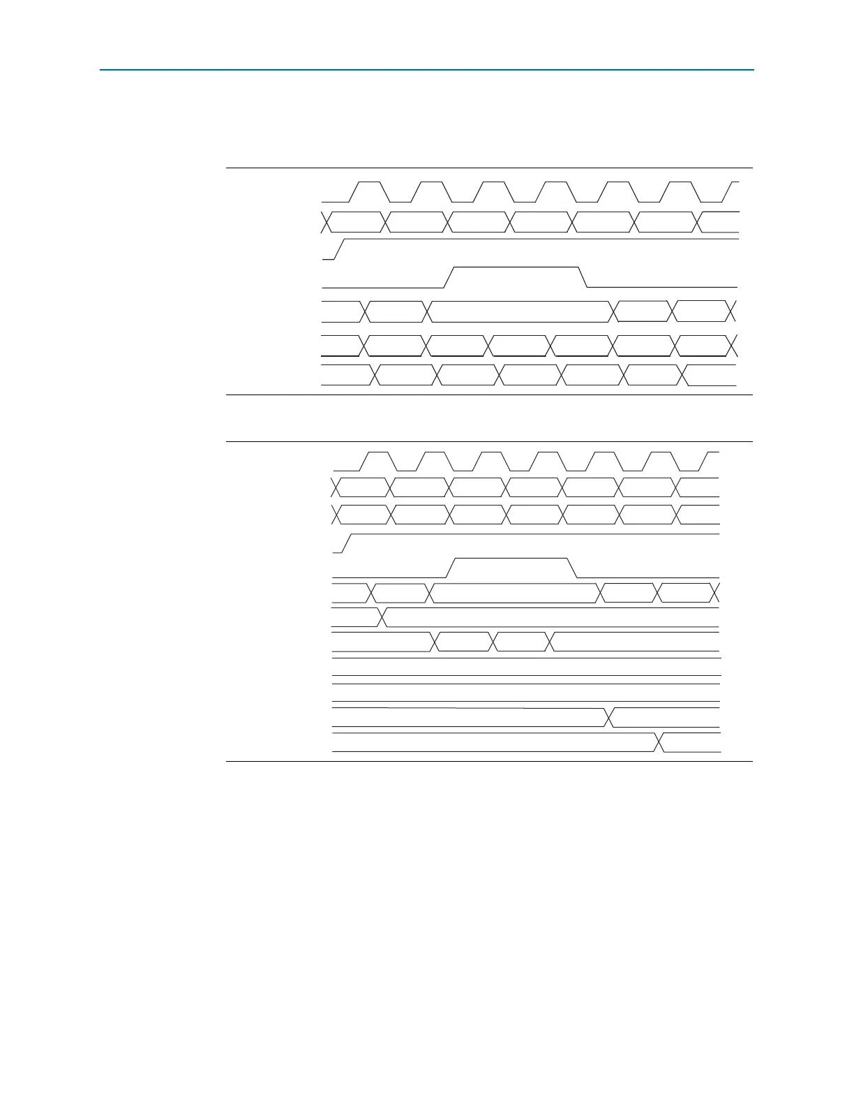
Figure 3–3 and Figure 3–4 show the address clock enable waveform during read and
write cycles, respectively.
Mixed-Width Support
M9K memory blocks support mixed data widths. When using simple dual-port, true
dual-port, or FIFO modes, mixed width support allows you to read and write
different data widths to an M9K memory block. For more information about the
different widths supported per memory mode, refer to “Memory Modes” on
page 3–7.
Figure 3–3. Cyclone IV Devices Address Clock Enable During Read Cycle Waveform
Figure 3–4. Cyclone IV Devices Address Clock Enable During Write Cycle Waveform
inclock
rden
rdaddress
q (synch)
a0 a1 a2 a3 a4 a5
a6
q (asynch)
an a0
a4
a5
latched address
(inside memory)
dout0
dout1
dout1
dout4
dout1
dout4
dout5
addressstall
a1
doutn-1
dout1
doutn
doutn
dout1
dout0
dout1
inclock
wren
wraddress
a0 a1 a2 a3 a4 a5
a6
an a0
a4 a5
latched address
(inside memory)
addressstall
a1
data
00
01 02
03 04
05
06
contents at a0
contents at a1
contents at a2
contents at a3
contents at a4
contents at a5
XX
04
XX
00
03
01
XX
02
XX
XX
XX
05