3–12 Chapter 3: Memory Blocks in Cyclone IV Devices
Memory Modes
Cyclone IV Device Handbook, November 2011 Altera Corporation
Volume 1
In true dual-port mode, you can access any memory location at any time from either
port A or port B. However, when accessing the same memory location from both
ports, you must avoid possible write conflicts. When you attempt to write to the same
address location from both ports at the same time, a write conflict happens. This
results in unknown data being stored to that address location. There is no conflict
resolution circuitry built into the Cyclone IV devices M9K memory blocks. You must
handle address conflicts external to the RAM block.
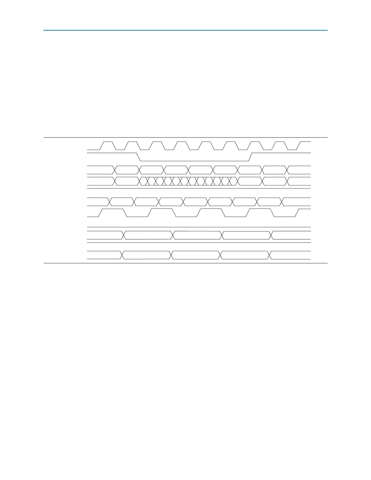
Figure 3–11 shows true dual-port timing waveforms for the write operation at port A
and read operation at port B. Registering the outputs of the RAM simply delays the
q
outputs by one clock cycle.
Shift Register Mode
Cyclone IV devices M9K memory blocks can implement shift registers for digital
signal processing (DSP) applications, such as finite impulse response (FIR) filters,
pseudo-random number generators, multi-channel filtering, and auto-correlation and
cross-correlation functions. These and other DSP applications require local data
storage, traditionally implemented with standard flipflops that quickly exhaust many
logic cells for large shift registers. A more efficient alternative is to use embedded
memory as a shift register block, which saves logic cell and routing resources.
The size of a (w× m×n) shift register is determined by the input data width (w), the
length of the taps (m), and the number of taps (n), and must be less than or equal to
the maximum number of memory bits, which is 9,216 bits. In addition, the size of
(w×n) must be less than or equal to the maximum width of the block, which is 36 bits.
If you need a larger shift register, you can cascade the M9K memory blocks.
Figure 3–11. Cyclone IV Devices True Dual-Port Timing Waveform
clk_a
wren_a
address_a
clk_b
an-1
an a0 a1 a2 a3 a4 a5
a6
q_b (asynch)
wren_b
address_b
bn
b0
b1 b2 b3
doutn-1
doutn
dout0
q_a (asynch)
din-1
din din4 din5 din6
data_a
din-1
din
dout0 dout1 dout2
dout3
din4
din5
dout2
dout1
rden_a
rden_b