Chapter 6: I/O Features in Cyclone IV Devices 6–11
I/O Standards
March 2016 Altera Corporation Cyclone IV Device Handbook,
Volume 1
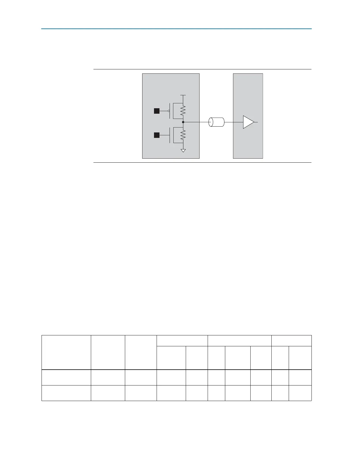
Figure 6–4 shows the single-ended I/O standards for OCT without calibration. The R
S
shown is the intrinsic transistor impedance.
All I/O banks and I/O pins support impedance matching and series termination.
Dedicated configuration pins and JTAG pins do not support impedance matching or
series termination.
R
S
OCT is supported on any I/O bank. V
CCIO
and V
REF
must be compatible for all I/O
pins to enable R
S
OCT in a given I/O bank. I/O standards that support different R
S
values can reside in the same I/O bank as long as their V
CCIO
and V
REF
do not conflict.
Impedance matching is implemented using the capabilities of the output driver and is
subject to a certain degree of variation, depending on the process, voltage, and
temperature.
f For more information about tolerance specification, refer to the Cyclone IV Device
Datasheet chapter.
I/O Standards
Cyclone IV devices support multiple single-ended and differential I/O standards.
Cyclone IV devices support 3.3-, 3.0-, 2.5-, 1.8-, 1.5-, and 1.2-V I/O standards.
Tab le 6 –3 summarizes I/O standards supported by Cyclone IV devices and which
I/O pins support them.
Figure 6–4. Cyclone IV Devices R
S
OCT Without Calibration
Cyclone IV Device
Driver Series Termination
Receiving
Device
V
CCIO
R
S
R
S
Z
O
GND
Table 6–3. Cyclone IV Devices Supported I/O Standards and Constraints (Part 1 of 3)
I/O Standard Type
Standard
Support
V
CCIO
Level (in V) Column I/O Pins Row I/O Pins
(1)
Input Output
CLK,
DQS
PLL_OUT
User
I/O
Pins
CLK,
DQS
User I/O
Pins
3.3-V LVTTL,
3.3-V LVCMOS
(2)
Single-ended JESD8-B
3.3/3.0/2.5
(3)
3.3 vv vvv
3.0-V LVTTL,
3.0-V LVCMOS
(2)
Single-ended JESD8-B
3.3/3.0/2.5
(3)
3.0 vv vvv