1–12 Chapter 1: Cyclone IV Device Datasheet
Operating Conditions
Cyclone IV Device Handbook, December 2016 Altera Corporation
Volume 3
Schmitt Trigger Input
Cyclone IV devices support Schmitt trigger input on the
TDI
,
TMS
,
TCK
,
nSTATUS
,
nCONFIG
,
nCE
,
CONF_DONE
, and
DCLK
pins. A Schmitt trigger feature introduces
hysteresis to the input signal for improved noise immunity, especially for signals with
slow edge rate. Table 1–14 lists the hysteresis specifications across the supported
V
CCIO
range for Schmitt trigger inputs in Cyclone IV devices.
I/O Standard Specifications
The following tables list input voltage sensitivities (V
IH
and V
IL
), output voltage (V
OH
and V
OL
), and current drive characteristics (I
OH
and I
OL
), for various I/O standards
supported by Cyclone IV devices. Table 1–15 through Table 1–20 provide the I/O
standard specifications for Cyclone IV devices.
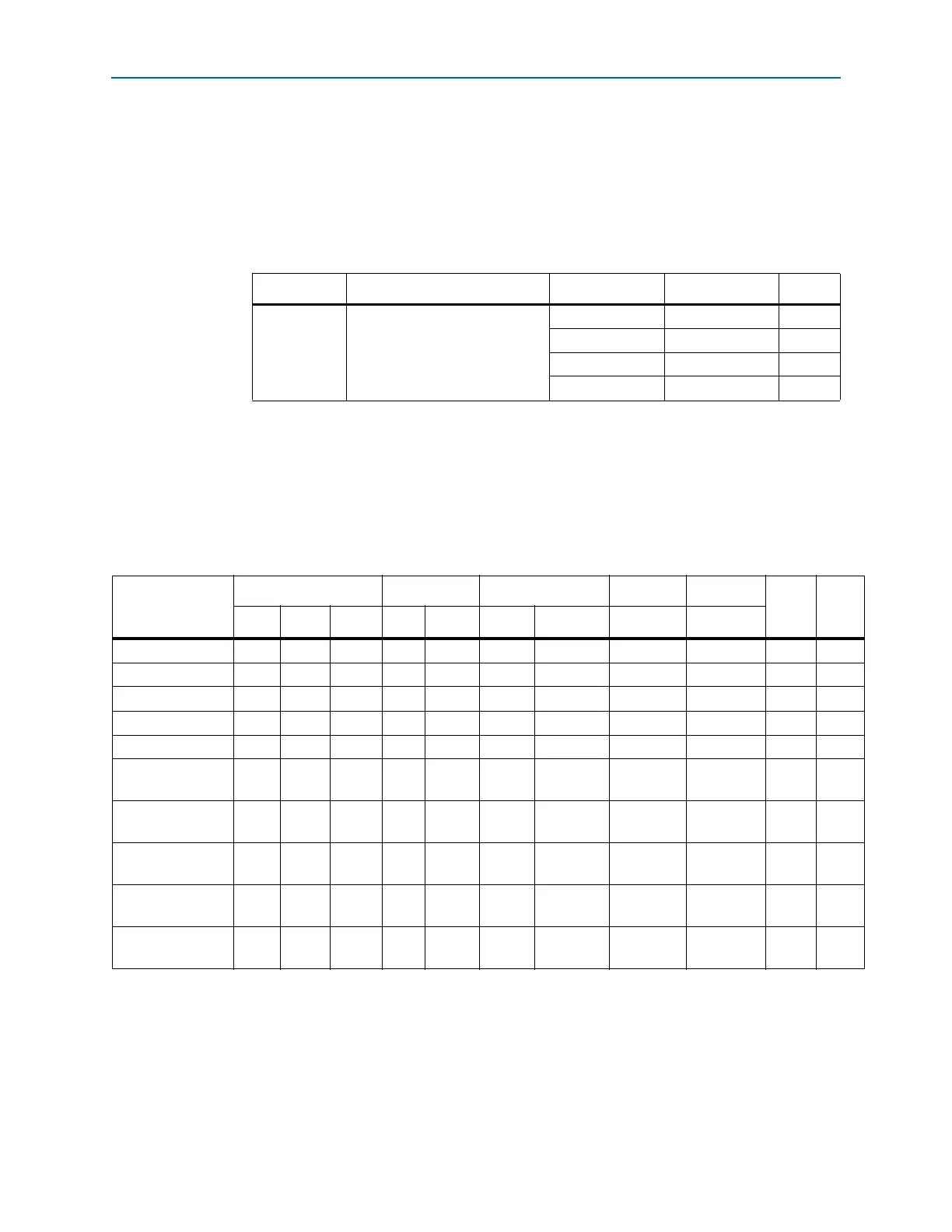
Table 1–14. Hysteresis Specifications for Schmitt Trigger Input in Cyclone IV Devices
Symbol Parameter Conditions (V) Minimum Unit
V
SCHMITT
Hysteresis for Schmitt trigger
input
V
CCIO
= 3.3 200 mV
V
CCIO
= 2.5 200 mV
V
CCIO
= 1.8 140 mV
V
CCIO
= 1.5 110 mV
Table 1–15. Single-Ended I/O Standard Specifications for Cyclone IV Devices
(1),
(2)
I/O Standard
V
CCIO
(V) V
IL
(V) V
IH
(V) V
OL
(V) V
OH
(V) I
OL
(mA)
(4)
I
OH
(mA)
(4)
Min Typ Max Min Max Min Max Max Min
3.3
-V LVTTL
(3)
3.135 3.3 3.465 — 0.8 1.7 3.6 0.45 2.4 4 –4
3.3
-V LVCMOS
(3)
3.135 3.3 3.465 — 0.8 1.7 3.6 0.2 V
CCIO
– 0.2 2 –2
3.0
-V LVTTL
(3)
2.85 3.0 3.15 –0.3 0.8 1.7 V
CCIO
+ 0.3 0.45 2.4 4 –4
3.0
-V LVCMOS
(3)
2.85 3.0 3.15 –0.3 0.8 1.7 V
CCIO
+ 0.3 0.2 V
CCIO
– 0.2 0.1 –0.1
2.5 V
(3)
2.375 2.5 2.625 –0.3 0.7 1.7 V
CCIO
+ 0.3 0.4 2.0 1 –1
1.8 V 1.71 1.8 1.89 –0.3
0.35 x
V
CCIO
0.65 x
V
CCIO
2.25 0.45
V
CCIO
–
0.45
2–2
1.5 V 1.425 1.5 1.575 –0.3
0.35 x
V
CCIO
0.65 x
V
CCIO
V
CCIO
+ 0.3
0.25 x
V
CCIO
0.75 x
V
CCIO
2–2
1.2 V 1.14 1.2 1.26 –0.3
0.35 x
V
CCIO
0.65 x
V
CCIO
V
CCIO
+ 0.3
0.25 x
V
CCIO
0.75 x
V
CCIO
2–2
3.0-V PCI 2.85 3.0 3.15 —
0.3 x
V
CCIO
0.5 x
V
CCIO
V
CCIO
+ 0.3 0.1 x V
CCIO
0.9 x V
CCIO
1.5 –0.5
3.0-V PCI-X 2.85 3.0 3.15 —
0.35 x
V
CCIO
0.5 x
V
CCIO
V
CCIO
+ 0.3 0.1 x V
CCIO
0.9 x V
CCIO
1.5 –0.5
Notes to Table 1–15:
(1) For voltage-referenced receiver input waveform and explanation of terms used in Table 1–15, refer to “Glossary” on page 1–37.
(2) AC load CL = 10 pF
(3) For more information about interfacing Cyclone IV devices with 3.3/3.0/2.5
-V LVTTL/LVCMOS I/O standards, refer to AN 447: Interfacing Cyclone III
and Cyclone IV Devices with 3.3/3.0/2.5-V LVTTL/LVCMOS I/O Systems.
(4) To meet the I
OL and IOH specifications, you must set the current strength settings accordingly. For example, to meet the 3.3-V LVTTL specification (4
mA), set the current strength settings to 4 mA or higher. Setting at lower current strength may not meet the I
OL and IOH specifications in the handbook.