Chapter 4: Embedded Multipliers in Cyclone IV Devices 4–3
Architecture
February 2010 Altera Corporation Cyclone IV Device Handbook,
Volume 1
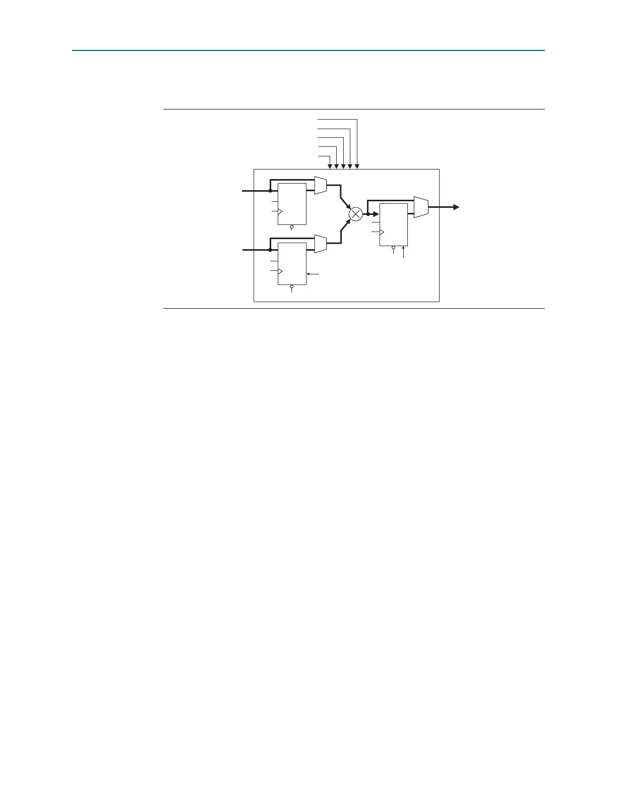
Figure 4–2 shows the multiplier block architecture.
Input Registers
You can send each multiplier input signal into an input register or directly into the
multiplier in 9- or 18-bit sections, depending on the operational mode of the
multiplier. You can send each multiplier input signal through a register independently
of other input signals. For example, you can send the multiplier
Data A
signal through
a register and send the
Data B
signal directly to the multiplier.
The following control signals are available for each input register in the embedded
multiplier:
■ clock
■ clock enable
■ asynchronous clear
All input and output registers in a single embedded multiplier are fed by the same
clock, clock enable, and asynchronous clear signals.
Multiplier Stage
The multiplier stage of an embedded multiplier block supports 9 × 9 or 18 × 18
multipliers, as well as other multipliers between these configurations. Depending on
the data width or operational mode of the multiplier, a single embedded multiplier
can perform one or two multiplications in parallel. For multiplier information, refer to
“Operational Modes” on page 4–4.
Each multiplier operand is a unique signed or unsigned number. The
signa
and
signb
signals control an input of a multiplier and determine if the value is signed or
unsigned. If the
signa
signal is high, the
Data A
operand is a signed number. If the
signa
signal is low, the
Data A
operand is an unsigned number.
Figure 4–2. Multiplier Block Architecture
CLRN
DQ
ENA
Data A
Data B
aclr
clock
ena
signa
signb
CLRN
DQ
ENA
CLRN
DQ
ENA
Data Out
Embedded Multiplier Block
Output
Register
Input
Register