Chapter 1: Cyclone IV FPGA Device Family Overview 1–3
Device Resources
March 2016 Altera Corporation Cyclone IV Device Handbook,
Volume 1
■ Up to 532 user I/Os
■ LVDS interfaces up to 840 Mbps transmitter (Tx), 875 Mbps Rx
■ Support for DDR2 SDRAM interfaces up to 200 MHz
■ Support for QDRII SRAM and DDR SDRAM up to 167 MHz
■ Up to eight phase-locked loops (PLLs) per device
■ Offered in commercial and industrial temperature grades
Device Resources
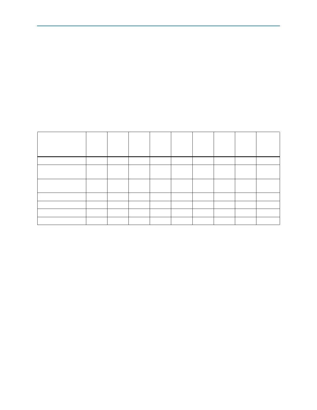
Tab le 1 –1 lists Cyclone IV E device resources.
Table 1–1. Resources for the Cyclone IV E Device Family
Resources
EP4CE6
EP4CE10
EP4CE15
EP4CE22
EP4CE30
EP4CE40
EP4CE55
EP4CE75
EP4CE115
Logic elements (LEs) 6,272 10,320 15,408 22,320 28,848 39,600 55,856 75,408 114,480
Embedded memory
(Kbits)
270 414 504 594 594 1,134 2,340 2,745 3,888
Embedded 18 × 18
multipliers
15 23 56 66 66 116 154 200 266
General-purpose PLLs22444444 4
Global Clock Networks 10 10 20 20 20 20 20 20 20
User I/O Banks 88888888 8
Maximum user I/O
(1)
179 179 343 153 532 532 374 426 528
Note to Table 1–1:
(1) The user I/Os count from pin-out files includes all general purpose I/O, dedicated clock pins, and dual purpose configuration pins. Transceiver
pins and dedicated configuration pins are not included in the pin count.