7–14 Chapter 7: External Memory Interfaces in Cyclone IV Devices
Cyclone IV Devices Memory Interfaces Features
Cyclone IV Device Handbook, March 2016 Altera Corporation
Volume 1
DDR Output Registers
A dedicated write DDIO block is implemented in the DDR output and output enable
paths.
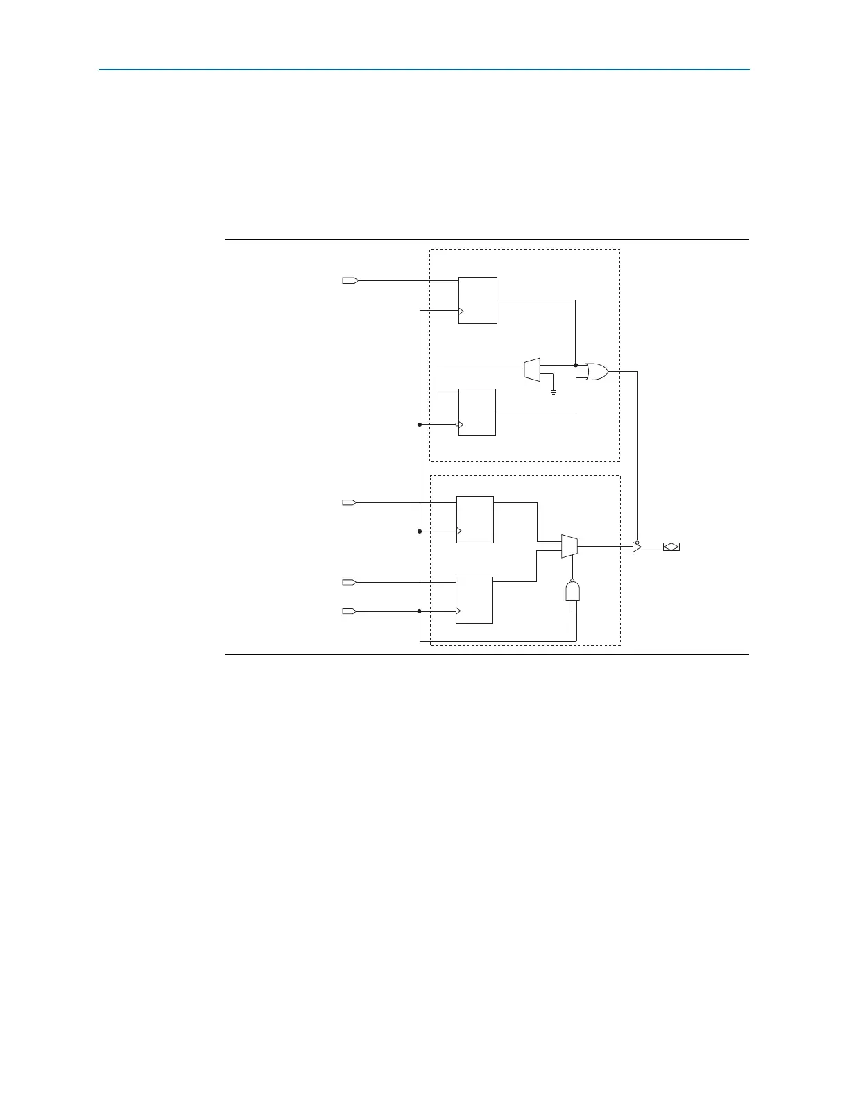
Figure 7–8 shows how a Cyclone IV dedicated write DDIO block is implemented in
the I/O element (IOE) registers.
The two DDR output registers are located in the I/O element (IOE) block. Two serial
data streams routed through
datain_l
and
datain_h
, are fed into two registers,
output
register Ao
and
output
register Bo
, respectively, on the same clock edge.
The output from
output
register Ao
is captured on the falling edge of the clock, while
the output from
output
register Bo
is captured on the rising edge of the clock. The
registered outputs are multiplexed by the common clock to drive the DDR output pin
at twice the data rate.
The DDR output enable path has a similar structure to the DDR output path in the
IOE block. The second output enable register provides the write preamble for the
DQS
strobe in DDR external memory interfaces. This active-low output enable register
extends the high-impedance state of the pin by half a clock cycle to provide the
external memory’s
DQS
write preamble time specification.
f For more information about Cyclone IV IOE registers, refer to the Cyclone IV Device
I/O Features chapter.
Figure 7–8. Cyclone IV Dedicated Write DDIO
IOE
Register
IOE
Register
Output Enable
-90° Shifted Clock
datain_l
Output Enable
Register A
OE
Output Enable
Register B
OE
data1
data0
IOE
Register
Output Register A
O
data0
data1
datain_h
IOE
Register
Output Register B
O
DDR Output Registers
DDR Output Enable Registers
DQ or DQS
®