Chapter 7: External Memory Interfaces in Cyclone IV Devices 7–13
Cyclone IV Devices Memory Interfaces Features
March 2016 Altera Corporation Cyclone IV Device Handbook,
Volume 1
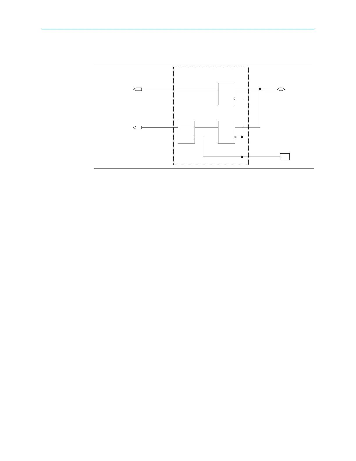
Figure 7–7 illustrates Cyclone IV DDR input registers.
These DDR input registers are implemented in the core of devices. The DDR data is
first fed to two registers, input register A
I
and input register B
I
.
■ Input register A
I
captures the DDR data present during the rising edge of the clock
■ Input register B
I
captures the DDR data present during the falling edge of the clock
■ Register C
I
aligns the data before it is synchronized with the system clock
The data from the DDR input register is fed to two registers,
sync_reg_h
and
sync_reg_l
, then the data is typically transferred to a FIFO block to synchronize the
two data streams to the rising edge of the system clock. Because the read-capture
clock is generated by the PLL, the read-data strobe signal (
DQS
or CQ) is not used
during read operation in Cyclone IV devices; hence, postamble is not a concern in this
case.
Figure 7–7. Cyclone IV DDR Input Registers
dataout_h
LE
Register
LE
Register
LE
Register
DQ
dataout_l
Input Register B
I
Input Register A
I
neg_reg_out
Register C
I
DDR Input Registers in Cyclone IV Device
Capture Clock
PLL