1–28 Chapter 1: Cyclone IV Transceivers Architecture
Transceiver Clocking Architecture
Cyclone IV Device Handbook, February 2015 Altera Corporation
Volume 2
The input reference clocks reside in banks 3A, 3B, 8A, and 8B have dedicated
V
CC_CLKIN3A
, V
CC_CLKIN3B
, V
CC_CLKIN8A
, and V
CC_CLKIN8B
power supplies separately in
their respective I/O banks to avoid the different power level requirements in the same
bank for general purpose I/Os (GPIOs). Table 1–6 lists the supported I/O standard
for the
REFCLK
pins.
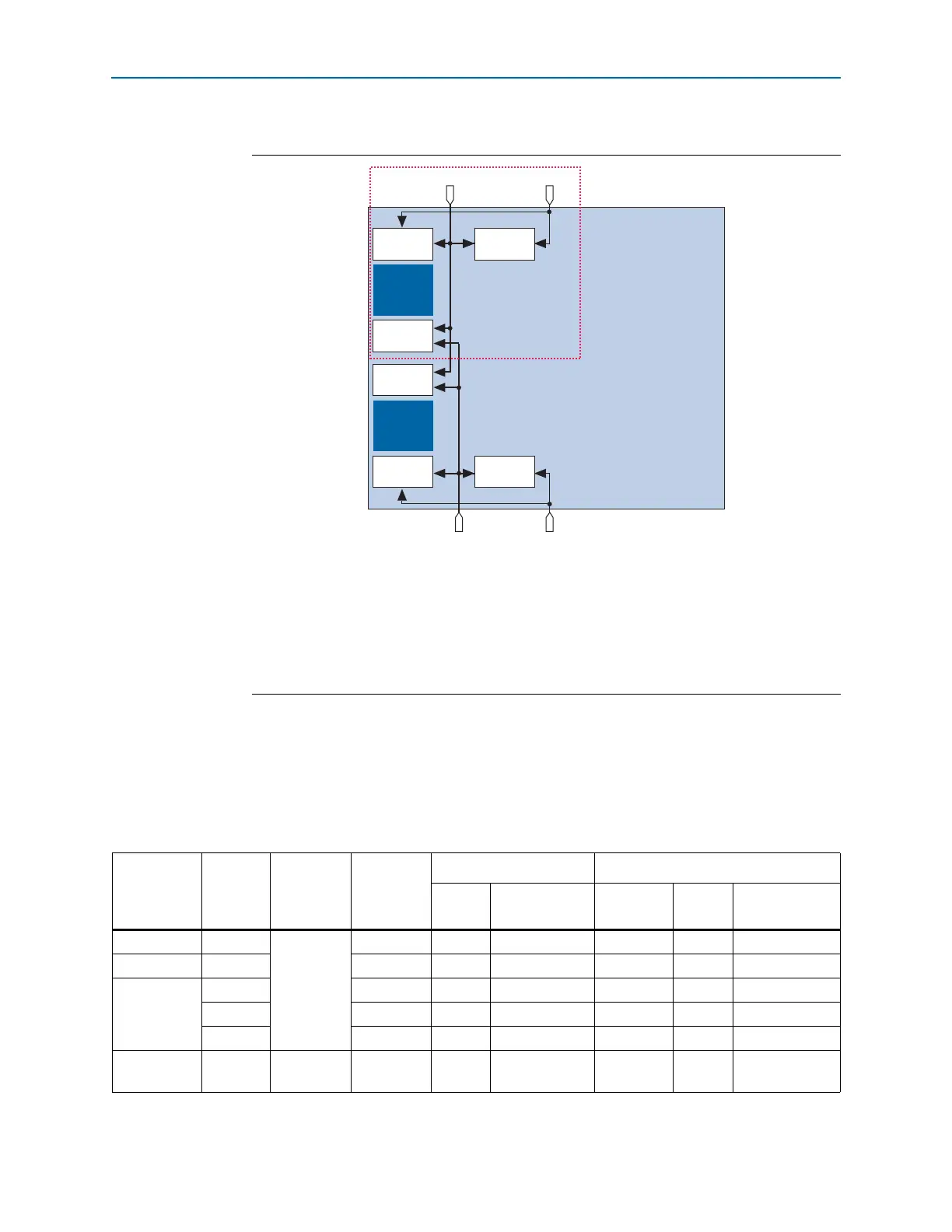
Figure 1–26. PLL Input Reference Clocks in Transceiver Operation for F484 and Larger Packages
(1)
,
(2)
,
(3)
Notes to Figure 1–26:
(1) The
REFCLK2
and
REFCLK3
pins are dual-purpose
CLKIO
,
REFCLK
, or
DIFFCLK
pins that reside in banks 3A and 8A
respectively.
(2) The
REFCLK[1..0]
and
REFCLK[5..4]
pins are dual-purpose differential
REFCLK
or
DIFFCLK
pins that reside in
banks 3B and 8B respectively. These clock input pins do not have access to the clock control blocks and GCLK
networks. For more details, refer to the Clock Networks and PLLs in Cyclone IV Devices chapter.
(3) Using any clock input pins other than the designated
REFCLK
pins as shown here to drive the MPLLs and GPLLs may
have reduced jitter performance.
Transceiver
Block
GXBL1
MPLL_8
REFCLK3
REFCLK[1..0]
MPLL_7
Transceiver
Block
GXBL0
MPLL_6
MPLL_5
REFCLK[5..4]
REFCLK2
GPLL_1
GPLL_2
Not applicable in
F484 package
Table 1–6. REFCLK I/O Standard Support
I/O Standard
HSSI
Protocol
Coupling
Terminatio
n
VCC_CLKIN Level I/O Pin Type
Input Output Column I/O Row I/O
Supported
Banks
LVDS ALL
Differential
AC (Needs
off-chip
resistor to
restore
V
CM
)
Off-chip 2.5 V Not Supported Yes No 3A, 3B, 8A, 8B
LVPECL ALL Off-chip 2.5 V Not Supported Yes No 3A, 3B, 8A, 8B
1.2 V, 1.5 V,
3.3 V PCML
ALL Off-chip 2.5 V Not Supported Yes No 3A, 3B, 8A, 8B
ALL Off-chip 2.5 V Not Supported Yes No 3A, 3B, 8A, 8B
ALL Off-chip 2.5 V Not Supported Yes No 3A, 3B, 8A, 8B
HCSL PCIe
Differential
DC
Off-chip 2.5 V Not Supported Yes No 3A, 3B, 8A, 8B