6–18 Chapter 6: I/O Features in Cyclone IV Devices
I/O Banks
Cyclone IV Device Handbook, March 2016 Altera Corporation
Volume 1
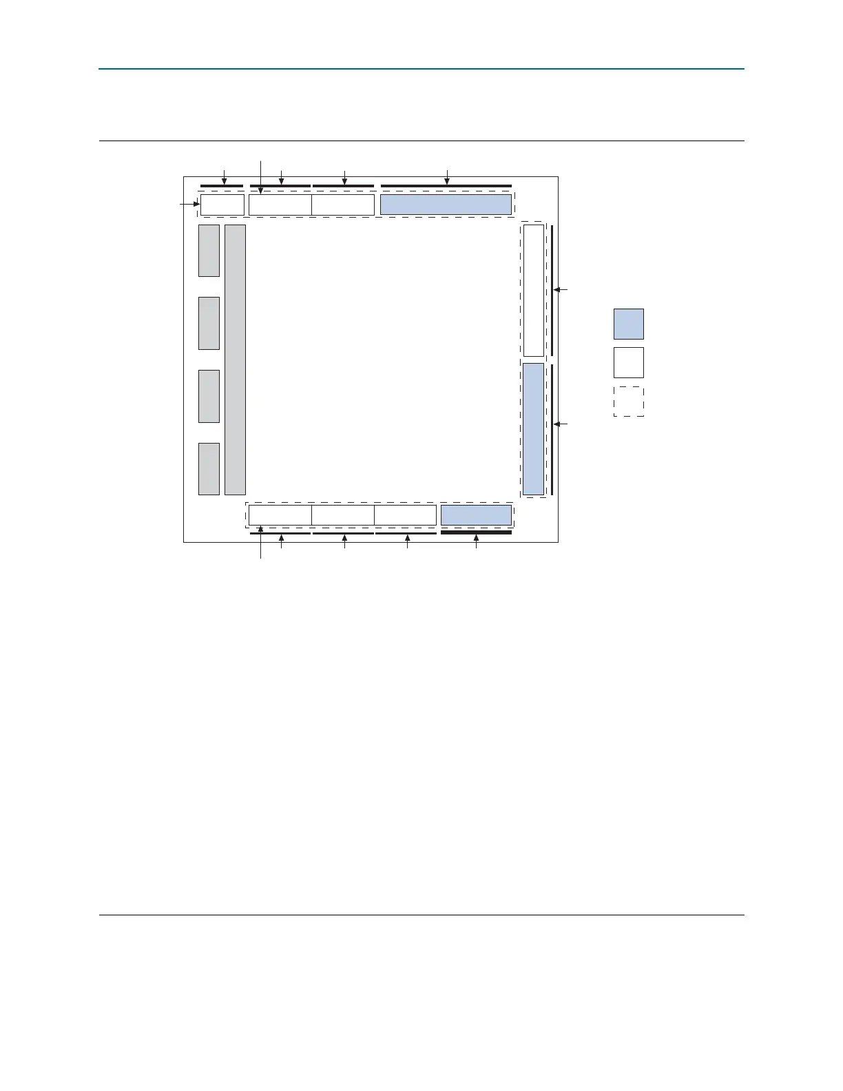
Figure 6–10 and Figure 6–11 show the overview of Cyclone IV GX I/O banks.
Figure 6–10. Cyclone IV GX I/O Banks for EP4CGX15, EP4CGX22, and EP4CGX30
(1),
(2),
(9)
Notes to Figure 6–10:
(1) This is a top view of the silicon die. For exact pin locations, refer to the pin list and the Quartus II software. Channels 2 and 3 are not available in
EP4CGX15 and F169 package type in EP4CGX22 and EP4CGX30 devices.
(2) True differential (PPDS, LVDS, mini-LVDS, and RSDS I/O standards) outputs are supported in row I/O banks 5 and 6 only. External resistors are
needed for the differential outputs in column I/O banks.
(3) The LVPECL I/O standard is only supported on clock input pins. This I/O standard is not supported on output pins.
(4) The HSTL-12 Class II is supported in column I/O banks 4, 7, and 8.
(5) The differential SSTL-18 and SSTL-2, differential HSTL-18, and HSTL-15 I/O standards are supported only on clock input pins and phase-locked
loops (PLLs) output clock pins. PLL output clock pins do not support Class II interface type of differential SSTL-18, HSTL-18, HSTL-15, and
HSTL-12 I/O standards.
(6) The differential HSTL-12 I/O standard is only supported on clock input pins and PLL output clock pins. Differential HSTL-12 Class II is supported
only in column I/O banks 4, 7, and 8.
(7) BLVDS output uses two single-ended outputs with the second output programmed as inverted. BLVDS input uses the LVDS input buffer.
(8) The PCI-X I/O standard does not meet the IV curve requirement at the linear region.
(9) The OCT block is located in the shaded banks 4, 5, and 7.
(10) There are two dedicated clock input I/O banks (I/O bank 3A and I/O bank 8A) that can be used for either high-speed serial interface (HSSI) input
reference clock pins or clock input pins.
(11) There are dual-purpose I/O pins in bank 9. If input pins with
VREF
I/O standards are used on these dual-purpose I/O pins during user mode, they
share the
VREF
pin in bank 8.These dual-purpose IO pins in bank 9 when used in user mode also support R
S
OCT without calibration and they
share the OCT block with bank 8.
(12) There are four dedicated clock input in I/O bank 3B for the EP4CGX30F484 device that can be used for either HSSI input reference clock pins or
clock input pins.
VCCIO9
Configuration
pins
Configuration pins
VCC_CLKIN3A
VCC_CLKIN3B
I/O Bank 3
I/O Bank
3A
(10)
I/O Bank 8
I/O Bank 9
(11)
I/O Bank
8A
(10)
Right, Top, and Bottom Banks Support:
3.3-V LVTTL/LVCMOS
3.0-V LVTTL/LVCMOS
2.5-V LVTTL/LVCMOS
1.8-V LVTTL/LVCMOS
1.5-V LVCMOS
1.2-V LVCMOS
PPDS
LVDS
RSDS
mini-LVDS
Bus LVDS (
7)
LVPECL
(3)
SSTL-2 class I and II
SSTL-18 Class I and II
HSTL-18 Class I and II
HSTL-15 Class I and II
HSTL-12 Class I and II
(4)
Differential SSTL-2
(5)
Differential SSTL-18
(5)
Differential HSTL-18
(5)
Differential HSTL-15
(5)
Differential HSTL-12
(6)
3.0-V PCI/PCI-X
(8)
VCCIO7
VCCIO6
VCCIO5
VCCIO4VCCIO3
Configuration pins
VCC_CLKIN8AVCCIO8
I/O Bank 7
I/O Bank 4
I/O Bank 5
PCIe hard IP x1, x2, and x4
I/O Bank 6
Channel 3Channel 2Channel 1Channel 0
I/O bank with
calibration block
I/O bank without
calibration block
Calibration block
coverage
I/O Bank
3B
(12)