Chapter 6: I/O Features in Cyclone IV Devices 6–17
I/O Banks
March 2016 Altera Corporation Cyclone IV Device Handbook,
Volume 1
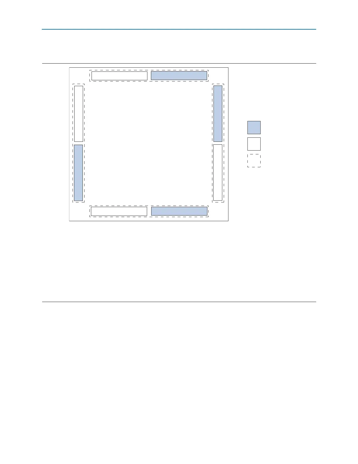
Figure 6–9 shows the overview of Cyclone IV E I/O banks.
Figure 6–9. Cyclone IV E I/O Banks
(1),
(2)
Notes to Figure 6–9:
(1) This is a top view of the silicon die. This is only a graphical representation. For exact pin locations, refer to the pin list and the Quartus II software.
(2) True differential (PPDS, LVDS, mini-LVDS, and RSDS I/O standards) outputs are supported in row I/O banks 1, 2, 5, and 6 only. External resistors
are needed for the differential outputs in column I/O banks.
(3) The LVPECL I/O standard is only supported on clock input pins. This I/O standard is not supported on output pins.
(4) The HSTL-12 Class II is supported in column I/O banks 3, 4, 7, and 8 only.
(5) The differential SSTL-18 and SSTL-2, differential HSTL-18, and HSTL-15 I/O standards are supported only on clock input pins and phase-locked
loops (PLLs) output clock pins. Differential SSTL-18, differential HSTL-18, and HSTL-15 I/O standards do not support Class II output.
(6) The differential HSTL-12 I/O standard is only supported on clock input pins and PLL output clock pins. Differential HSTL-12 Class II is supported
only in column I/O banks 3, 4, 7, and 8.
(7) BLVDS output uses two single-ended outputs with the second output programmed as inverted. BLVDS input uses true LVDS input buffer.
All I/O Banks Support:
3.3-V LVTTL/LVCMOS
3.0-V LVTTL/LVCMOS
2.5-V LVTTL/LVCMOS
1.8-V LVTTL/LVCMOS
1.5-V LVCMOS
1.2-V LVCMOS
PPDS
LVDS
RSDS
mini-LVDS
Bus LVDS (
7)
LVPECL
(3)
SSTL-2 class I and II
SSTL-18 CLass I and II
HSTL-18 Class I and II
HSTL-15 Class I and II
HSTL-12 Class I and II
(4)
Differential SSTL-2
(5)
Differential SSTL-18
(5)
Differential HSTL-18
(5)
Differential HSTL-15
(5)
Differential HSTL-12
(6)
I/O Bank 8 I/O Bank 7
I/O Bank 3 I/O Bank 4
I/O Bank 2
I/O Bank 1
I/O Bank 5
I/O Bank 6
I/O bank with
calibration block
I/O bank without
calibration block
Calibration block
coverage