Chapter 6: I/O Features in Cyclone IV Devices 6–27
High-Speed I/O Interface
March 2016 Altera Corporation Cyclone IV Device Handbook,
Volume 1
Table 6–8 and Table 6–9 summarize the total number of supported row and column differential channels in the Cyclone IV
device family.
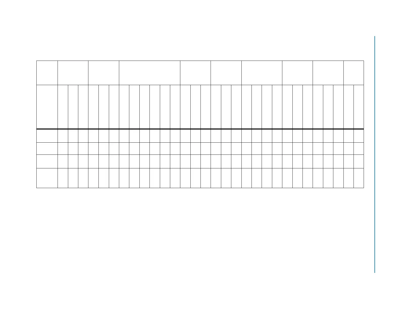
Table 6–8. Cyclone IV E I/O and Differential Channel Count
Device
EP4CE6
EP4CE10
EP4CE15
EP4CE22
EP4CE30
EP4CE40
EP4CE55
EP4CE75
EP4CE115
Numbers of Differential
Channels
(1), (2)
144-EQPF
256-UBGA
256-FBGA
144-EQPF
256-UBGA
256-FBGA
144-EQPF
164-MBGA
256-MBGA
256-UBGA
256-FBGA
484-FBGA
144-EQPF
256-UBGA
256-FBGA
324-FBGA
484-FBGA
780-FBGA
324-FBGA
484-UBGA
484-FBGA
780-FBGA
484-UBGA
484-FBGA
780-FBGA
484-UBGA
484-FBGA
780-FBGA
484-FBGA
780-FBGA
User
I/O
(3)
91 179 179 91 179 179 81 89 165 165 165 343 79 153 153 193 328 532 193 328 328 532 324 324 374 292 292 426 280 528
User I/O
Banks
888888888888888888888888888888
LVDS
(4), (
6)
8 23 23 8 23 23 6 8 21 21 21 67 7 20 20 30 60 112 30 60 60 112 62 62 70 54 54 79 50 103
Emulated
LVDS
(5), (
6)
13 43 43 13 43 43 12 13 32 32 32 70 10 32 32 38 64 112 38 64 64 112 70 70 90 56 56 99 53 127
Notes to Table 6–8:
(1) User I/O pins are used as inputs or outputs; clock input pins are used as inputs only; clock output pins are used as output only.
(2) For differential pad placement guidelines, refer to “Pad Placement” on page 6–23.
(3) The I/O pin count includes all GPIOs, dedicated clock pins, and dual-purpose configuration pins. Dedicated configuration pins are not included in the pin count.
(4) The true LVDS count includes all LVDS I/O pairs, differential clock input and clock output pins in row I/O banks 1, 2, 5, and 6.
(5) The emulated LVDS count includes all LVDS I/O pairs, differential clock input and clock output pins in column I/O banks 3, 4, 7, and 8.
(6) LVDS input and output buffers are sharing the same p and n pins. One LVDS I/O channel can only be either transmitter or receiver at a time.