Chapter 5: Clock Networks and PLLs in Cyclone IV Devices 5–17
Clock Networks
October 2012 Altera Corporation Cyclone IV Device Handbook,
Volume 1
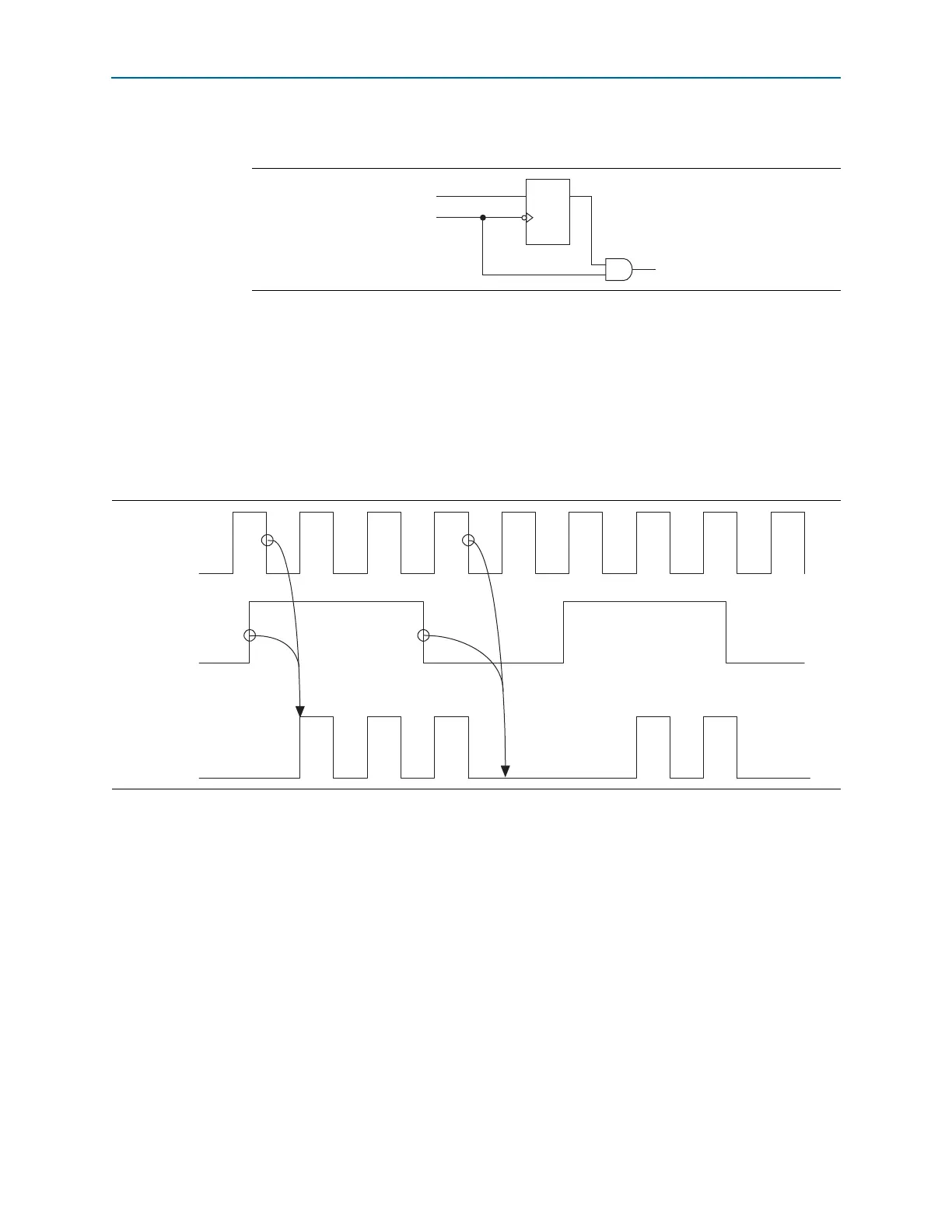
Figure 5–7 shows how to implement the
clkena
signal with a single register.
1 The
clkena
circuitry controlling the output C0 of the PLL to an output pin is
implemented with two registers instead of a single register, as shown in Figure 5–7.
Figure 5–8 shows the waveform example for a clock output enable. The
clkena
signal
is sampled on the falling edge of the clock (
clkin
).
1 This feature is useful for applications that require low power or sleep mode.
The
clkena
signal can also disable clock outputs if the system is not tolerant to
frequency overshoot during PLL resynchronization.
Altera recommends using the
clkena
signals when switching the clock source to the
PLLs or the GCLK. The recommended sequence is:
1. Disable the primary output clock by de-asserting the
clkena
signal.
2. Switch to the secondary clock using the dynamic select signals of the clock control
block.
3. Allow some clock cycles of the secondary clock to pass before reasserting the
clkena
signal. The exact number of clock cycles you must wait before enabling the
secondary clock is design-dependent. You can build custom logic to ensure
glitch-free transition when switching between different clock sources.
Figure 5–7. clkena Implementation
DQ
clkena clkena_out
clk_ou
clkin
Figure 5–8. clkena Implementation: Output Enable