1–40 Chapter 1: Cyclone IV Device Datasheet
Glossary
Cyclone IV Device Handbook, December 2016 Altera Corporation
Volume 3
T
t
C
High-speed receiver and transmitter input and output clock period.
Channel-to-
channel-skew
(TCCS)
High-speed I/O block: The timing difference between the fastest and slowest output edges,
including t
CO
variation and clock skew. The clock is included in the TCCS measurement.
t
cin
Delay from the clock pad to the I/O input register.
t
CO
Delay from the clock pad to the I/O output.
t
cout
Delay from the clock pad to the I/O output register.
t
DUTY
High-speed I/O block: Duty cycle on high-speed transmitter output clock.
t
FALL
Signal high-to-low transition time (80–20%).
t
H
Input register hold time.
Timing Unit
Interval (TUI)
High-speed I/O block: The timing budget allowed for skew, propagation delays, and data
sampling window. (TUI = 1/(Receiver Input Clock Frequency Multiplication Factor) = t
C
/w).
t
INJITTER
Period jitter on the PLL clock input.
t
OUTJITTER_DEDCLK
Period jitter on the dedicated clock output driven by a PLL.
t
OUTJITTER_IO
Period jitter on the general purpose I/O driven by a PLL.
t
pllcin
Delay from the PLL inclk pad to the I/O input register.
t
pllcout
Delay from the PLL inclk pad to the I/O output register.
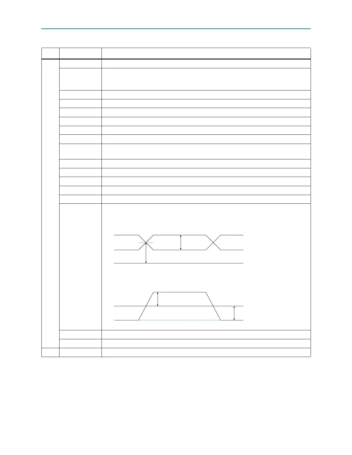
Transmitter
Output
Waveform
Transmitter output waveforms for the LVDS, mini-LVDS, PPDS and RSDS Differential I/O
Standards:
t
RISE
Signal low-to-high transition time (20–80%).
t
SU
Input register setup time.
U ——
Table 1–46. Glossary (Part 4 of 5)
Letter Term Definitions
Single-Ended Waveform
Differential Waveform (Mathematical Function of Positive & Negative Channel)
Positive Channel (p) = V
OH
Negative Channel (n) = V
OL
Ground
V
OD
V
OD
V
OD
0 V
V
os
p - n