128 KByte Flash Module (S12FTMRG128K1V1)
MC9S12G Family Reference Manual Rev.1.27
NXP Semiconductors 1039
All possible P-Flash protection scenarios are shown in Figure 29-14 . Although the protection scheme is
loaded from the Flash memory at global address 0x3_FF0C during the reset sequence, it can be changed
by the user. The P-Flash protection scheme can be used by applications requiring reprogramming in single
chip mode while providing as much protection as possible if reprogramming is not required.
2
FPLDIS
Flash Protection Lower Address Range Disable — The FPLDIS bit determines whether there is a
protected/unprotected area in a specific region of the P-Flash memory beginning with global address 0x3_8000.
0 Protection/Unprotection enabled
1 Protection/Unprotection disabled
1–0
FPLS[1:0]
Flash Protection Lower Address Size — The FPLS bits determine the size of the protected/unprotected area
in P-Flash memory as shown in Table 29-20. The FPLS bits can only be written to while the FPLDIS bit is set.
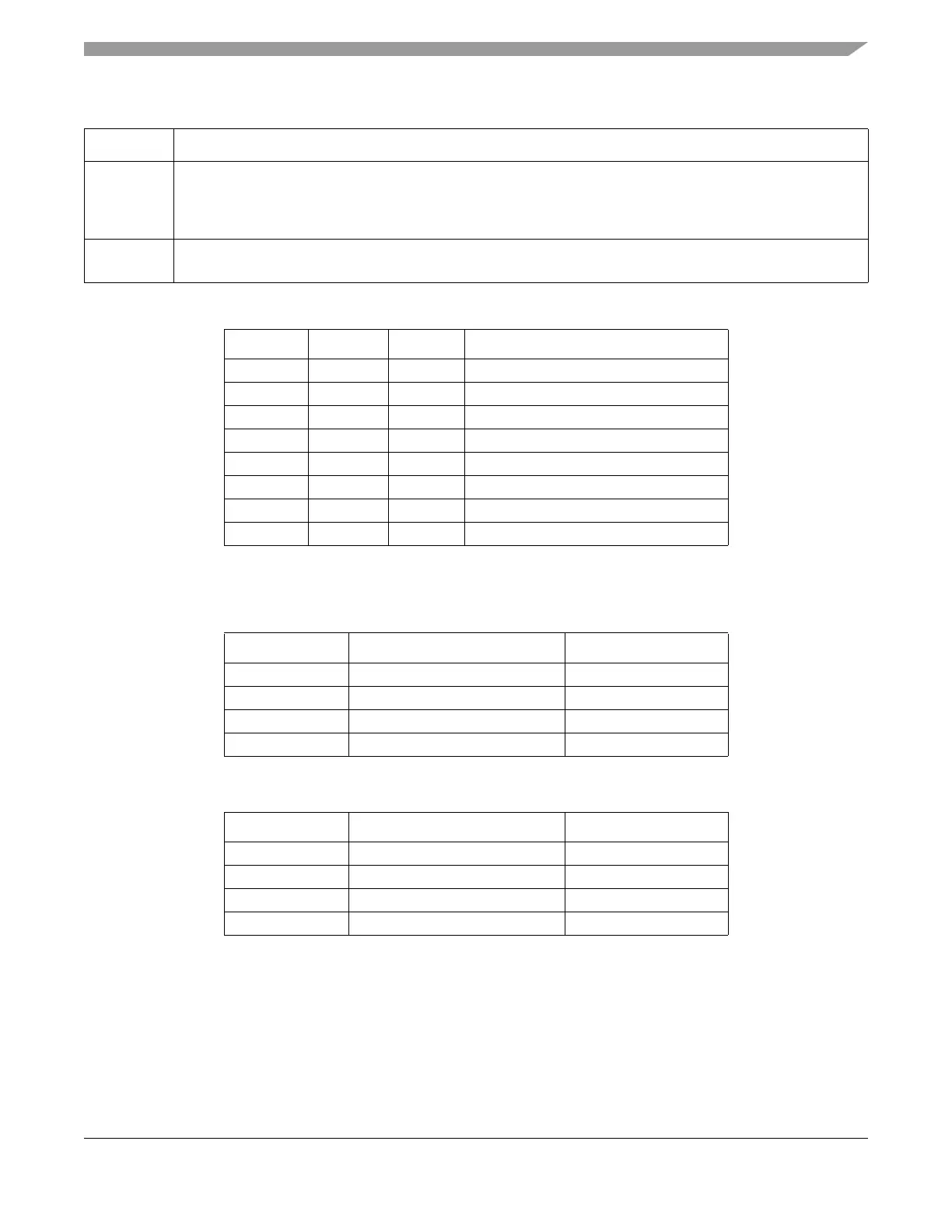
Table 29-18. P-Flash Protection Function
FPOPEN FPHDIS FPLDIS Function
1
1
For range sizes, refer to Table 29-19 and Table 29-20.
1 1 1 No P-Flash Protection
1 1 0 Protected Low Range
1 0 1 Protected High Range
1 0 0 Protected High and Low Ranges
0 1 1 Full P-Flash Memory Protected
0 1 0 Unprotected Low Range
0 0 1 Unprotected High Range
0 0 0 Unprotected High and Low Ranges
Table 29-19. P-Flash Protection Higher Address Range
FPHS[1:0] Global Address Range Protected Size
00 0x3_F800–0x3_FFFF 2 Kbytes
01 0x3_F000–0x3_FFFF 4 Kbytes
10 0x3_E000–0x3_FFFF 8 Kbytes
11 0x3_C000–0x3_FFFF 16 Kbytes
Table 29-20. P-Flash Protection Lower Address Range
FPLS[1:0] Global Address Range Protected Size
00 0x3_8000–0x3_83FF 1 Kbyte
01 0x3_8000–0x3_87FF 2 Kbytes
10 0x3_8000–0x3_8FFF 4 Kbytes
11 0x3_8000–0x3_9FFF 8 Kbytes
Table 29-17. FPROT Field Descriptions (continued)
Field Description

 Loading...


