240 KByte Flash Module (S12FTMRG240K2V1)
MC9S12G Family Reference Manual Rev.1.27
1136 NXP Semiconductors
31.3.2.2 Flash Security Register (FSEC)
The FSEC register holds all bits associated with the security of the MCU and Flash module.
All bits in the FSEC register are readable but not writable.
During the reset sequence, the FSEC register is loaded with the contents of the Flash security byte in the
Flash configuration field at global address 0x3_FF0F located in P-Flash memory (see Table 31-4) as
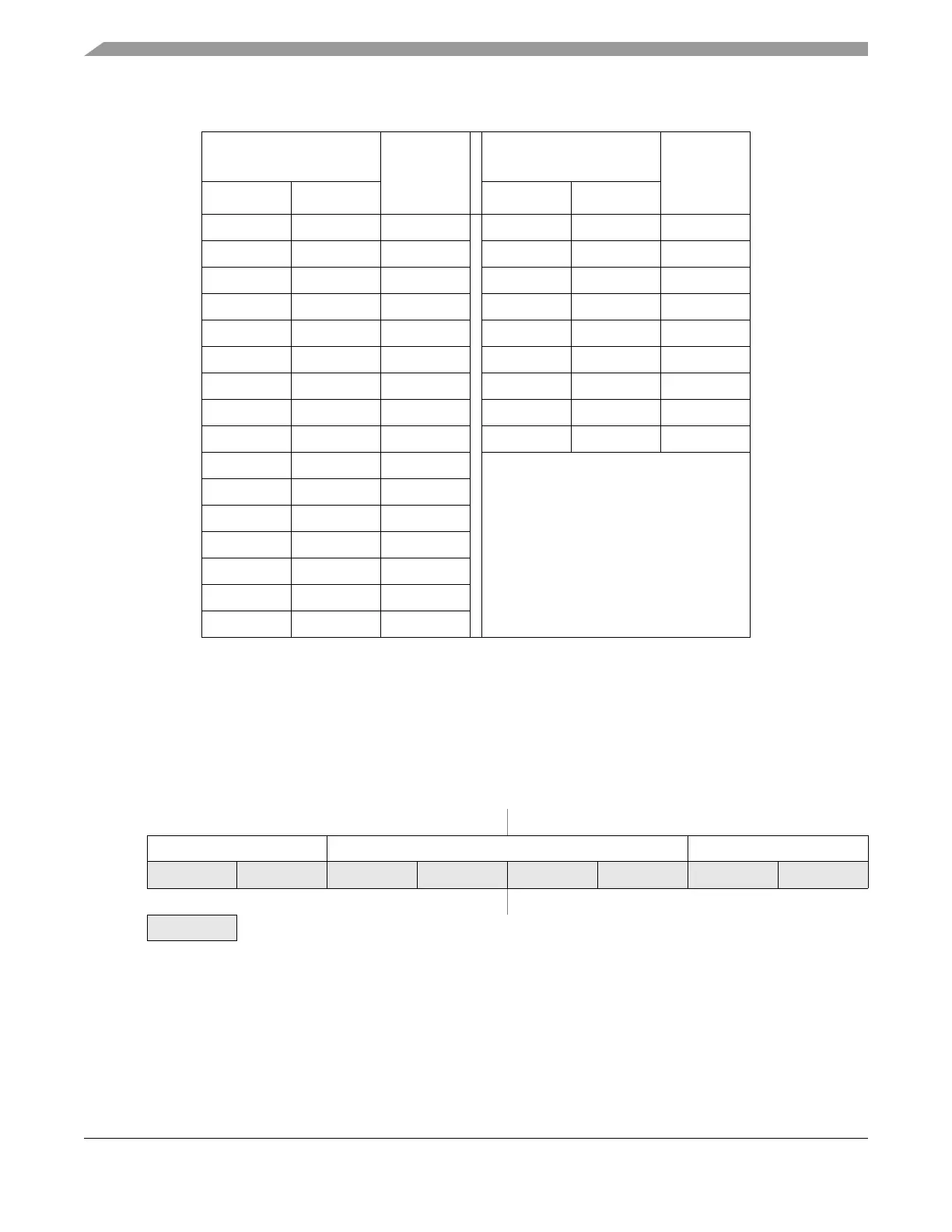
Table 31-8. FDIV values for various BUSCLK Frequencies
BUSCLK Frequency
(MHz)
FDIV[5:0]
BUSCLK Frequency
(MHz)
FDIV[5:0]
MIN
1
1
BUSCLK is Greater Than this value.
MAX
2
2
BUSCLK is Less Than or Equal to this value.
MIN
1
MAX
2
1.0 1.6 0x00 16.6 17.6 0x10
1.6 2.6 0x01 17.6 18.6 0x11
2.6 3.6 0x02 18.6 19.6 0x12
3.6 4.6 0x03 19.6 20.6 0x13
4.6 5.6 0x04 20.6 21.6 0x14
5.6 6.6 0x05 21.6 22.6 0x15
6.6 7.6 0x06 22.6 23.6 0x16
7.6 8.6 0x07 23.6 24.6 0x17
8.6 9.6 0x08 24.6 25.6 0x18
9.6 10.6 0x09
10.6 11.6 0x0A
11.6 12.6 0x0B
12.6 13.6 0x0C
13.6 14.6 0x0D
14.6 15.6 0x0E
15.6 16.6 0x0F
Offset Module Base + 0x0001
76543210
R KEYEN[1:0] RNV[5:2] SEC[1:0]
W
Reset F
1
1
Loaded from IFR Flash configuration field, during reset sequence.
F
1
F
1
F
1
F
1
F
1
F
1
F
1
= Unimplemented or Reserved
Figure 31-6. Flash Security Register (FSEC)

 Loading...


